( Please post if you spot errors / any corrections )
Oscillator …Internal 64Mhz was set in configuration . Note ..Default seems to be LVP = ON so MCLRE = EXTMCLR
Code:
#pragma config FEXTOSC = OFF // External Oscillator Selection (Oscillator not enabled)
#pragma config RSTOSC = HFINTOSC_64MHZ// Reset Oscillator Selection (HFINTOSC with HFFRQ = 64 MHz and CDIV = 1:1)
// CONFIG1H
#pragma config CLKOUTEN = OFF // Clock out Enable bit (CLKOUT function is disabled)
#pragma config PR1WAY = ON // PRLOCKED One-Way Set Enable bit (PRLOCK bit can be cleared and set only once)
#pragma config CSWEN = ON // Clock Switch Enable bit (Writing to NOSC and NDIV is allowed)
#pragma config FCMEN = ON // Fail-Safe Clock Monitor Enable bit (Fail-Safe Clock Monitor enabled)

// CONFIG2L
#pragma config MCLRE = EXTMCLR // MCLR Enable bit (If LVP = 0, MCLR pin function is port defined function; If LVP =1, RE3 pin fuction is MCLR)
#pragma config PWRTS = PWRT_OFF // Power-up timer selection bits (PWRT is disabled)
#pragma config MVECEN = ON // Multi-vector enable bit (Multi-vector enabled, Vector table used for interrupts)
#pragma config IVT1WAY = ON // IVTLOCK bit One-way set enable bit (IVTLOCK bit can be cleared and set only once)
#pragma config LPBOREN = OFF // Low Power BOR Enable bit (ULPBOR disabled)
#pragma config BOREN = SBORDIS // Brown-out Reset Enable bits (Brown-out Reset enabled , SBOREN bit is ignored)
// CONFIG2H
#pragma config BORV = VBOR_2P45 // Brown-out Reset Voltage Selection bits (Brown-out Reset Voltage (VBOR) set to 2.45V)
#pragma config ZCD = OFF // ZCD Disable bit (ZCD disabled. ZCD can be enabled by setting the ZCDSEN bit of ZCDCON)
#pragma config PPS1WAY = ON // PPSLOCK bit One-Way Set Enable bit (PPSLOCK bit can be cleared and set only once; PPS registers remain locked after one clear/set cycle)
#pragma config STVREN = ON // Stack Full/Underflow Reset Enable bit (Stack full/underflow will cause Reset)
#pragma config DEBUG = OFF // Debugger Enable bit (Background debugger disabled)
#pragma config XINST = OFF // Extended Instruction Set Enable bit (Extended Instruction Set and Indexed Addressing Mode disabled)
// CONFIG3L
#pragma config WDTCPS = WDTCPS_31// WDT Period selection bits (Divider ratio 1:65536; software control of WDTPS)
#pragma config WDTE = OFF // WDT operating mode (WDT Disabled; SWDTEN is ignored)
// CONFIG3H
#pragma config WDTCWS = WDTCWS_7// WDT Window Select bits (window always open (100%); software control; keyed access not required)
#pragma config WDTCCS = SC // WDT input clock selector (Software Control)
// CONFIG4L
#pragma config BBSIZE = BBSIZE_512// Boot Block Size selection bits (Boot Block size is 512 words)
#pragma config BBEN = OFF // Boot Block enable bit (Boot block disabled)
#pragma config SAFEN = OFF // Storage Area Flash enable bit (SAF disabled)
#pragma config WRTAPP = OFF // Application Block write protection bit (Application Block not write protected)
// CONFIG4H
#pragma config WRTB = OFF // Configuration Register Write Protection bit (Configuration registers (300000-30000Bh) not write-protected)
#pragma config WRTC = OFF // Boot Block Write Protection bit (Boot Block (000000-0007FFh) not write-protected)
#pragma config WRTD = OFF // Data EEPROM Write Protection bit (Data EEPROM not write-protected)
#pragma config WRTSAF = OFF // SAF Write protection bit (SAF not Write Protected)
#pragma config LVP = ON // Low Voltage Programming Enable bit (Low voltage programming enabled. MCLR/VPP pin function is MCLR. MCLRE configuration bit is ignored)
// CONFIG5L
#pragma config CP = OFF // PFM and Data EEPROM Code Protection bit (PFM and Data EEPROM code protection disabled)

#include <xc.h>
#include <string.h>
#include <stdlib.h>
#define _XTAL_FREQ 64000000
void OSC_init() , was coded for perhaps future changes.
Delays... XC8 Has some built in delays , for example __delay_ms(100); __delay_us(100);
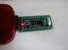
Xtal frequency has to be defined as above ... A led / 470R was put on RB5 and the delays were tested … all good.
Before establishing UART1 Serial, ( 2 available ) the PSS feature has to be understood , turns out is remarkably comprehensive and straight forward... and possibly more advanced than other PIC's (Note only digital can be multiplexed via PSS).
Note PPS registers have a locking feature as per data sheet.
PSS...Output..
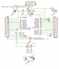
Step 1 . Where do I want the U1TX pin , RB6, RB7 are ICSP and the LED was on RB5, so RB4 .
The PPS ( output ) has registers RxyPPS , for the 8 bit of the A,B,C ports so RB4PPS points to pin, to assign U1TX the value from the RxyPSS table ( Data Sheet * ) is coded …. ( any B or C port pins could have been used )
[ 6'b01 0011 UART1 (TX) - B C ]
PSS...Input.
From Data Sheet
-------------------------------------------------------------------------------------
REGISTER 19-1: xxxPPS: PERIPHERAL xxx INPUT SELECTION
bit 7-5
Unimplemented: Read as ‘0’
bit 4-3
xxxPPS<4:3>: Peripheral xxx Input PORTx Pin Selection bits
See Table 19-1 for the list of available ports and default pin locations.
11 = Reserved
10 = PORTC
01 = PORTB
00 = PORTA
bit 2-0
xxxPPS<2:0>: Peripheral xxx Input PORTx Pin Selection bits
111 = Peripheral input is from PORTx Pin 7 (Rx7)
110 = Peripheral input is from PORTx Pin 6 (Rx6)
101 = Peripheral input is from PORTx Pin 5 (Rx5)
100 = Peripheral input is from PORTx Pin 4 (Rx4)
011 = Peripheral input is from PORTx Pin 3 (Rx3)
010 = Peripheral input is from PORTx Pin 2 (Rx2)
001 = Peripheral input is from PORTx Pin 1 (Rx1)
000 = Peripheral input is from PORTx Pin 0 (Rx0)
---------------------------------------------------------------------------------------
PPS Inputs are logically reverse of outputs. The peripheral input has the register and the value assigns the pin via the xxxPPS table. U1 receive PPS register = b'01011 for RB3 pin.
The respective TRIS bits were set in the IO_init()
Result so far …
Code:
void OSC_init(){

OSCFRQ=0x08; // 8=64 Mhz----0=1Mhz

}

void IO_init(){
ANSELA=0; // all digital
ANSELB=0; // all digital
ANSELC=0; // all digital
TRISBbits.TRISB5=0; // led
TRISBbits.TRISB4=0; // U1TX
TRISBbits.TRISB3=1; // U1RX
LATBbits.LATB5=1; // Turns the led on
}

void PPS_init(){
RB4PPS=0x13; // RB4 = UART1 TX.
U1RXPPS=0x0B; // RB3 = UART1 RX
}
( I come from machine code so use HEX a lot ! )
Break here to solder on a FTDI and swat up on UART ....
Note , After reading the mountain of K42 'Features' it is obvious I will not be able to cover everything. The idea was more of a launch pad, to see the mcu's project possibilities.


")


 I just now see there are 19 registers associated with I2C ..... See you next year


