Continue to Site

Welcome to our site!

Electro Tech is an online community (with over 170,000 members) who enjoy talking about and building electronic circuits, projects and gadgets. To participate you need to register. Registration is free. Click here to register now.

  • Welcome to our site! Electro Tech is an online community (with over 170,000 members) who enjoy talking about and building electronic circuits, projects and gadgets. To participate you need to register. Registration is free. Click here to register now.

PCB Fabrication: Fusion PCB v. Elecrow v. Smart-Prototyping

Status
Not open for further replies.
Has anyone used either Fusion PCB, Elecrow, Smart-Prototyping recently? A search here appears that some folks have used Elecrow or Smart-Prototyping in the past and the reviews appeared to be favorable.

How about Fusion PCB?

All three have a 100mmx100mm quantity of 10 offer for the exact same $4.90US. What gives with the pricing?

P.S. I do realize I am inquiring during Chinese New Year.
 
I believe that all of the low cost boards are coming from a couple different factories. Elecrow, Smart Prototyping, etc., arrange the panels I believe and the boards are made by the same factory.

I was gathering evidence to support this theory by looking at the batch number put on each set of boards. Boards from several of the vendors had the same format number, and a couple others had a different format. Most boards don't have these batch numbers any more so I don't have any solid conclusions but I believe this to be true.

I have recently had boards made by Smart Prototyping and Elecrow. Both provided high quality boards; I wasn't pushing the technology with 8 mil space and trace.

If you are using these services, I definitely recommend using DHL Shenzhen shipping. From Elecrow, you'll have boards in hand in 7 or 8 days. A batch of 10 boards is about $17 to ship, but you can add several more batches or other products to that shipment for little or no increase in cost.

I have had Elecrow do turnkey assembly on a few boards. The quality was excellent but not without problems.

The first set of boards had 2 sip resistor packages. In my mind, it was clear that the mark on the package should go near the mark on the board. They very consistently did not see it that way - every one was backwards. Spell out the details for the orientation of all parts, even you you are certain it's obvious. This was a batch of 25 through hole boards, so it wasn't too difficult to correct.

The second batch of boards was 60 small SMT boards with a number of ICs. We were hit with counterfeit parts on this lot. A Linear Technology I2C programmable oscillator chip would happily response to any and all messages on the I2C bus, no matter what address they were intended for. I don't fault Elecrow for this as the chips were visually indistinguishable from the real thing. They reworked the boards at no charge when I sent them back with known-good parts. I had a stressful week or two waiting for the boards to arrive in China, shipped via USPS. I asked DHL for the cost to return the boards - their answer was "more than the cost of the original assembled boards."

One other option I have used is Juvtmall.com. They price tbeir boards at $25 for "urgent + shipping" for a batch of ten 100mm x 100mm boards. If you are making only one batch of boards, this is about a wash with Elecrow. If you are making more, this quickly becomes more expensive.
 
By the way, Elecrow handle slots and cutouts just fine - I included them on the Gerber mechanicsl layer and got exactly what I expected.

I have also made black cover panels - sandwich a board between two blank panels with stsndoffs as a low-cost enclosure. Include a note saying there are no traces or components on the board and ALL the Gerber layers, blank or not and everything will go smotthly. If you don't include all layers, there will ne delays because they will think you forgot to include an essential layer.
 
I also noticed with these three services, it appears that you (the designer) can submit panelized gerber files up to a maximum size increment (one of the increments being 100mm x 100mm). Ie., you can panelize two of the same 40mm x 90mm boards on the 100mm x 100mm size increment for no cost increase. They also give you instructions on how to do this with the warning that you are responsible for cutting the boards apart. There is an upcharge if you panelize two different designs in the same gerber set.
 
I have also made black cover panels - sandwich a board between two blank panels with stsndoffs as a low-cost enclosure.
When I worked next door to a PCB house, I walked across the street and asked for a sheet of fiber class to make a box with. No problem.
Asking a PCB house across the internet to make a PCB with out copper is a real problem. I put a logo on the PCB and label the pieces. (logo in copper) "Power in", "HDMI" in copper will work with out questions.
You need copper or they will not make the board. "inside", "top edge", "bottom edge", "front", "back"//Then on the outside put the logo.


Not true for Elecrow. I have 2 boards on my desk that I had made with no copper at all. One of them is a 100mm x 100mm cover panel thst goes over a GPS antennna. Copper would have interfered with that.

As I said, Elecrow has been very accomodating. A note explaining that the board has no copper plus the Gerber files for the empty copper layers and the boards were made with no questions asked. If you don't include the files, they will assume you forgot to include them; this will evoke an email discussion, slowing the process down.

I do two things with every batch of boards. I send a readme file listing the board size, layers, files names and so forth along with comments about odd features like unplated holes, milled slots and cutouts and things like no copper or silkscreen layers. I don't know if this is ever read, but the details are there if anybody looks.

The second thing I do is to include the board outline on every Gerber layer. This ensures that progress doesn't stop because they don't notice the board outline on a single layer. It may also help Eagle with "empty" copper layers - no, it does not result in a ring of copper around the board perimeter.
 
I also noticed with these three services, it appears that you (the designer) can submit panelized gerber files up to a maximum size increment (one of the increments being 100mm x 100mm). Ie., you can panelize two of the same 40mm x 90mm boards on the 100mm x 100mm size increment for no cost increase. They also give you instructions on how to do this with the warning that you are responsible for cutting the boards apart. There is an upcharge if you panelize two different designs in the same gerber set.

The rules on multiple designs on one panel (not limited to 100mm x 100mm) are always changing. From personal experience, with board prices at 50 cents each, I would not "depanelize" my own boards. I have done so in the past were Advanced Circuits had their "3 for $33" specials for like an 8" x 10" panel (note that this was 3 panels for $33 EACH), but times have changed. If you saw boards apart, you create a cloud of abrasive, irritating dust. Shearing boards apart works ok (get a tile shear at the home improvement store) but rough edges and irregular boards will probably be a result. At least make your life easier if you do thing and arrange cut lines all the way from edge to edge.

Elecrow and others do offer v-score and other panelizing options. This is great for boards you will have professionally assembled or if you have a small board you need many of. V-scored boards snap apart, but you are left with a rough edge rather than a smooth machined edge. Also, there is not option to round corners when you do this.
 
I'm looking at using the Elecrow service. How do you specify a slot or cutout? (Please try to keep the instructions as generic as possible, I will likely need to translate into Protel 99SE)
 
You need to show slots and cutouts on a Gerber mechanical layer, usually with the extension GML.

In Eagle, you show the slot/cutout in layer 46, the milling layer. The CAM includes this layer in the GML. The picture below shows the mechanical layer. The outline is the board outline. The two rounded rectangles are cutouts. The outline of 8 non-plated holes are also shown.

The Eagle CAM section is shown below. I don't know how this translates into your software.

I also include a readme file with the Gerbers, explaining there are slots and cutouts.


gerber gml layer.png


GML Cam.jpg
 
Why would the NPTH be shown in the mechanical gerber? I haven't looked but I don't think Protel 99SE does it that way. They only show up in the Drill Drawing and the legend designates them as not being plated. I will double check this all tomorrow.
 
I don't know why they show up in the mechanical layer but it doesn't appear to be a problem.

Elecrow does request a NPTH (non-plated through hole) layer for non-plated holes. When I have only non-plated holes and no milling, I only include the NPTH layer and not the GML layer.

I am away from my computer; I can't remember exactly how I create the NPTH layer.
 
Been a really really long time since I used Protel.

On the package I use now it hasn't been an issue for me. I just simply place a slot on my board, or several holes to form a slot and generate the RS-274-X gerbers. Send them off to Elecrow, they contact you if they dont understand anything.

EDIT: I'll add for cutouts or routing I'd place on a mechanical layer and label it "routed"
 
Somehow in 20 years, I have not had to have internal openings in a board. I have made some very strangely shaped ones, but always solid center.

When the follow the board edge outline, they stay to the outside edge. If I place a "board edge" line in the middle of the board on the mechanical layer, will they stay to the inside. OK. That might be confusing. How about an example:

I want to make a circular board (a donut), 2" radius with a 1" radius hole (the resulting board should be just 1" wide). I place two circles on the mechanical layout, (one at 1" radius, one a 2" radius).

Do I end up with a the board I described, or is it narrow by the diameter of the bit because the center hole was cut to the same side (outside) of the line as the outside edge of the board?

I also cannot recall when the last time was I had a hole that was not plated. All of my mounting holes are plated and padded. This keeps the mounting hardware from chewing up the board and forces the layout to maintain enough clearance for the outside diameter of the mounting hardware. (for example see Arduino UNO, they have a hole that can just barely be used because the connector is too close to it)
 
I don't know why they show up in the mechanical layer but it doesn't appear to be a problem.

Elecrow does request a NPTH (non-plated through hole) layer for non-plated holes. When I have only non-plated holes and no milling, I only include the NPTH layer and not the GML layer.

I am away from my computer; I can't remember exactly how I create the NPTH layer.

Looks like I will have to research this. I don't see an obvious option for for adding NPTH to any layer.

Eagle has a layer specific for NPTH?

...I only include the NPTH layer and not the GML layer.
 
Last edited:
What I would do here is create a square board, place a 4mm routing groove around your board with the words "route" to show what to do. For each routed section use 4mm unplated holes at the starts and ends, but keep a gap between them to hold your board in place. See pic attached for what I mean, explain it all on a mech layer, hopefully it makes sense.
 

Attachments

  • donut pcb.png
    donut pcb.png
    14.4 KB · Views: 189
No. Whatever shape you want the board to be, draw that as the board outline. Rectangular, rectangular with rounded corners, round, in the pattern of an oakleaf. Just remember, it is routed, so any inside corners will have some radius.

For your round hole, make a circle of the diameter you want it to be. Done.

For your inside cutout, draw a circle in the mechanical layer with the diameter you want the hole to be.

For slots, I draw the perimeter of the slot I want,without any allowance for cutter size and without any drills involved. I have gotten exactly what I wanted when I've done this.

I will post some examples shortly.
 
No need for the examples. I follow. Draw what I want and be done with it. If I want a donut, then draw the two concentric circles and submit.

With that being said, I read Elecrow has a minimum slot width of 1mm (due to a bit diameter of 0.8mm).

I'm still trying to figure out if there is a way to get Protel 99SE to show the NPTH hole on the mechanical layer without manually place a circle on the mechanical layer coincident with the drill hole (then having to manage both from then on).
 
I feel like posting pictures :)

This is the package drawing for a DC power connector. I followed somebody else's lead on this, and put slots within the hole/pad. You can see thin blue lines defining the slot.
DC Power Jack.jpg
This is the round board made with this package.
Round DC Jack Board.jpg
And finally, the result. It's difficult to tell, but the slots are plated.
round board.jpg

Here's another PCB footprint for mounting INA219 current sense modules. Functionally identical modules come in two sizes, so I used slots to accommodate the mounting screws for either version. The blue lines define the slots and the finished boards using this footprint reflect this exactly. The hashed lines represent copper restrict areas for fills, as I didn't want these slots plated, but this may not actually be necessary - see next example.
INA219.jpg

The last example is a spacer board I made. As above, blue lines show the slots. These boards have copper fills but the slots are not plated without any special effort on my part.
spacer.jpg
The boards do not have plated slots.
spacer board.jpg

The CAM processor for my NPTH layer has only the dimension layer and hole layer included, without the drills layer. It pops up a message every time asking if it's ok that holes are selected but drills are not but only non-plated holes show up in the output. The top and bottom copper layers have neither drills nor holes included. Give this a try and see what happens.
 
The CAM processor for my NPTH layer has only the dimension layer and hole layer included, without the drills layer. It pops up a message every time asking if it's ok that holes are selected but drills are not but only non-plated holes show up in the output. The top and bottom copper layers have neither drills nor holes included. Give this a try and see what happens.

I just cannot find a way to do this. I do not see any options that allows a gerber file to be generated with circles for the holes.

upload_2018-2-15_15-31-46.png


I can generate the drill drawing (third tab) that has differently shaped same size symbols for the drill locations (uses .Legend to show the drill sizes). I can also generate a drill guide (fourth tab) that has varying + symbols for each hole (does not indicate the specific hole size just where and may be different size).

I have 14 mechanical layers, 16 internal planes, and 30 mid layers I can add, but nothing that is specific for showing only the NPTH holes. If I (have to) do this it looks like it will have to be done manually. (unless someone recalls how to do this in Protel 99SE)

However, I did find a way to include the board outline on each layer without having to draw it on each layer (a setting on the Mech Layers tab #5). :) 
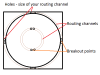
Now the mounting pads are too close to the keep out line which on top and bottom will turn into copper. :( Looks like I have some squishing to do.

Update: Moving the board outline so it shows up on all layers had a negative side effect. Although it prints on the keep out layer, it isn't on the keep out layer so no design rules to the board edge are enforced. :( Looks like I have to have the board outline on two layers, a mechanical layer and the keep out layer, if I want the auto router to stay in bounds and the board outline to show in all gerber files.
 
Last edited:
Status
Not open for further replies.

Latest threads

New Articles From Microcontroller Tips

Back
Top