Continue to Site

Welcome to our site!

Electro Tech is an online community (with over 170,000 members) who enjoy talking about and building electronic circuits, projects and gadgets. To participate you need to register. Registration is free. Click here to register now.

  • Welcome to our site! Electro Tech is an online community (with over 170,000 members) who enjoy talking about and building electronic circuits, projects and gadgets. To participate you need to register. Registration is free. Click here to register now.

Output voltage a bit low and switching noise at high loads on this SMPS

Status
Not open for further replies.

FusionITR

Member
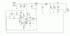
Ok, I made a PCB and built this circuit and it works just fine. However, the output voltage is suppose to be 5V and at light load it ouputs 4.9V and at full load (1A) it outputs about 4.82V. Is 0.08V decent load regulation or is that pretty poor? Also, is there any reason why the light load output voltage is 0.1V off of the intended voltage? I used 1% resistors everywhere in the feedback network. Where can I check in the circuit to see where the problem is?

Also, at loads approximently greater than 0.3A, if I put my ear really close to the circuit, I can kinda hear switching noises, probably from the transistor or inductor. Is there normal? Is there anyway to supress this?

Thanks.
Schematic for the circuit is attached.
 

Attachments

  • schematic.gif
    schematic.gif
    55.4 KB · Views: 443
0.1V at 5V is 2%, so your error is only two percent, simply alter the feedback values to give you exactly 5V - if that's what you want?. Likewise your regulation is 2%, is that a problem?. As for noise, inductors in SMPS's commonly make a noise, increase the frequency until it's too high to hear!, or use a better inductor.
 
A couple of things about your converter...

The TL5001 has a reference voltage accuracy of 3%, so your output is actually well within the bounds of the guaranteed spec without taking into account the added stack up of the 1% resistors.

Your feedback network is not good. You have a voltage divider set up (R5 and R4) prior to the compensation network. To be honest, I don't even know what this will do to the network. The way to set the voltage without messing with the compensation network is to place the voltage set resistor from the Feedback pin of the regulator IC to ground. This method assures that the ac component is not affected (in the small signal ac analysis, the feedback node is shorted to ground which removes that resistor from the analysis completely).

In regards to the compensation network - I would suspect that this system is not stable. I would suggest the following changes:
R5 - short this with a jumper
R4 - leave open (do not populate)
R1 - change to 12.1 kOhms (1%)
R2 - change to 215 Ohms (1%)
R6 - change to 12.1 kOhms (1%)
C3 - change to 15nF
C4 - change to 330pF
C5 - change to 33nF (please take note of the n's and p's)
Now place a 3.01k (1%) resistor between Pin 4 (VFB) and Ground.

These values made some assumptions regarding the inductor DCR and output capacitor ESR, but it should provide a much more stable system than what you have now.

I would suggest the following read through to get a better understanding of stabilizing voltage mode buck regulators...

https://www.electro-tech-online.com/custompdfs/2006/07/tb417.pdf
 
Nigel Goodwin said:
0.1V at 5V is 2%, so your error is only two percent, simply alter the feedback values to give you exactly 5V - if that's what you want?. Likewise your regulation is 2%, is that a problem?. As for noise, inductors in SMPS's commonly make a noise, increase the frequency until it's too high to hear!, or use a better inductor.

Thanks, I just wanted to know if those regulation values were acceptable for a pratical design since im new to power supplies. Typically, would choosing a pwm with a voltage reference of 1% error and using 0.1% resistors help in getting an exact voltage I want without adjusting the feedback resistors?

Also, as far as the switching noise, is the only way to decrease the noise is to use a better inductor? When looking at an inductor datasheet, what specification do I need to look out for?
 
OutToLunch said:
Your feedback network is not good. You have a voltage divider set up (R5 and R4) prior to the compensation network. To be honest, I don't even know what this will do to the network. The way to set the voltage without messing with the compensation network is to place the voltage set resistor from the Feedback pin of the regulator IC to ground. This method assures that the ac component is not affected (in the small signal ac analysis, the feedback node is shorted to ground which removes that resistor from the analysis completely).

In regards to the compensation network - I would suspect that this system is not stable. I would suggest the following changes:
R5 - short this with a jumper
R4 - leave open (do not populate)
R1 - change to 12.1 kOhms (1%)
R2 - change to 215 Ohms (1%)
R6 - change to 12.1 kOhms (1%)
C3 - change to 15nF
C4 - change to 330pF
C5 - change to 33nF (please take note of the n's and p's)
Now place a 3.01k (1%) resistor between Pin 4 (VFB) and Ground.

These values made some assumptions regarding the inductor DCR and output capacitor ESR, but it should provide a much more stable system than what you have now.

I would suggest the following read through to get a better understanding of stabilizing voltage mode buck regulators...

https://www.electro-tech-online.com/custompdfs/2006/07/tb417-1.pdf

Thanks for your obversations on my feedback compensation network. I choose those values based on the type 3 feedback compensation and the gain plot of my output inductor and my capacitors and their ESR ratings (gain plot taken from spice simulations).

I'll look at document you gave me to see if I can improve my understanding of feedback compensation to make my design more stable.

Is there anyway I can test the stablibilty of my feedback compensation?
 
FusionITR said:
Is there anyway I can test the stablibilty of my feedback compensation?
The expensive way is with a network analyzer that would inject a small ac signal into the loop and spit out a bode plot of gain and phase.

The easy way to do it would be to apply a transient load and examine the response of the output voltage. If the output settles rather quickly without too much overshoot or ring, then it's cool. The only problem with this method is that if there is a stability problem it's harder to root out which components you should modify to get the response you require.
 
FusionITR said:
Thanks, I just wanted to know if those regulation values were acceptable for a pratical design since im new to power supplies. Typically, would choosing a pwm with a voltage reference of 1% error and using 0.1% resistors help in getting an exact voltage I want without adjusting the feedback resistors?

Also, as far as the switching noise, is the only way to decrease the noise is to use a better inductor? When looking at an inductor datasheet, what specification do I need to look out for?

This is a power supply, not a precision reference. You don't need better than 5% for powering circuits. Anything better will be a big waste of money.

Switch mode power supplies generate both radiated and conducted noise. "better inductor" whatever that means (shielded?), likely only addresses radiated noise. Conducted noise can be dealt with by filtering.

Also, layout of your high current loops can make or break your design noise-wise.
 
OutToLunch said:
The easy way to do it would be to apply a transient load and examine the response of the output voltage. If the output settles rather quickly without too much overshoot or ring, then it's cool. The only problem with this method is that if there is a stability problem it's harder to root out which components you should modify to get the response you require.

Whats the best way to apply a transient load? Would using a mos transistor in the triode region work by applying a square wave signal to the base to turn the transistor on and off very rapidly? Maybe the mosfet in series with another resistor to apply a load then remove the load?

Something like this:

**broken link removed**

Would that be a good way to test?
 
Optikon said:
This is a power supply, not a precision reference. You don't need better than 5% for powering circuits. Anything better will be a big waste of money.

Switch mode power supplies generate both radiated and conducted noise. "better inductor" whatever that means (shielded?), likely only addresses radiated noise. Conducted noise can be dealt with by filtering.

Also, layout of your high current loops can make or break your design noise-wise.

What kind of filtering for the conducted noise?
 
Yes, you could apply a repetitive load in the manner you have shown. I would go for a maximum load step - from no load to full load and then analyze the response.

If you want to filter your output voltage even more, just use another LC filter.
 
FusionITR said:
What kind of filtering for the conducted noise?

Some high frequency ceramic types on your output would be a start. Those 100uF electrolytics have very high series R and series L making them unsuitable for filtering high frequency switching noise. They only work well near DC as reservoir capacitors for the load. Switching transients will go right by them.
 
Optikon said:
Some high frequency ceramic types on your output would be a start. Those 100uF electrolytics have very high series R and series L making them unsuitable for filtering high frequency switching noise. They only work well near DC as reservoir capacitors for the load. Switching transients will go right by them.

What made you assume they are electrolytics?

They are low esr tantalum capacitors, datasheet here: https://www.electro-tech-online.com/custompdfs/2006/07/TPS20Series.pdf

The input capacitors are also low esr tantalums.
 
How unreliable? Meaning they have a short life span or are prone to premature failure?

Also, if you don't recommend tantalums, what do you recommend?
 
FusionITR said:
How unreliable? Meaning they have a short life span or are prone to premature failure?

Also, if you don't recommend tantalums, what do you recommend?

I would use 105 degree low ESR electrolytics, and probably put small ceramics across them as well (I would for tantalums as well).

In my experience tantalums have a great tendency to go S/C in a fairly short time, a common fault finding technique is to look and see if there are any tantalums on the board - check them before you do anything else. It's extremely rare to see them in domestic electronics these days, there was a stage when they were popular, but their poor reliability led to them been dropped.
 
FusionITR said:
How unreliable? Meaning they have a short life span or are prone to premature failure?

Also, if you don't recommend tantalums, what do you recommend?

I think it is OK to keep your tantalums (tantalums are electrolytic) but you really need ceramic types also. Ceramic types if properly located will maintain low impedance well into the 10's MHz region - right where you need it with your switching transients. The same cannot be said for some tantalums (low ESR or not). Remember, consider the impedance of the capacitors at high frequencies not just at the frequency they were tested at (on datasheet = ESR spec)

If you are worried about premature failure (they are prone as pointed out) there is something you can do about that. I've found if you sufficiently derate them in the design, they CAN work reliably.

For derating, most important is probably voltage. The more the better. I would do at least 2X. I.e. max volts = 10V I would use a 25V rated.

Next is ripple current. You'll have to calculate or measure this in circuit under highest load conditions. I would derate this one by at least 2X also.
If you can model the capacitor correctly, simulation comes in very handy for this.

Last is temperature, if the unit will operate within say 20% of max temperature, I would bump it up to a higher grade. I have a feeling, this is not going to be an issue for your design though.
 
When you say put small ceramics across them, do you mean a ceramic in parallel before the main electrolytic/tantalum filter caps? What would be a good size? 0.1uF?
 
FusionITR said:
When you say put small ceramics across them, do you mean a ceramic in parallel before the main electrolytic/tantalum filter caps? What would be a good size? 0.1uF?

Yes right at the output of your inductor. 0.1uF or 0.01uF C0G/NP0/X7R types would be fine. In the physical construction, this should be located literally right at the output of the inductor.

High frequency noise voltage will pass through the inductor but will be shunted by the capacitor that you are adding.

Also, it is helpful to trace out high frequency current loops on your schematic. Use a high-lighter or something. Then, when you build this circuit (or layout in CAD tools) make sure that this "loop" is physically as small as possible (minimize its area).

Doing this will also help with noise.
 
Ceramic capacitors, when used in conjunction with bulk capacitors, are generally placed at or as close to the point of load to provide immediate load support during a fast transient (i.e. high load current slew rates). The bulks are there to help support the rail while the inductor slews up. As far as needing them in this regulator, I don't see impementing them as hurting anything, but I don't think they're going to add much either. The output current maxes out at 1A - no transient this regulator will see will be enough to deplete the charge in the output caps prior to the inductor slewing up.
 
Ok I did some testing with the stablization (using the schematic I posted earlier, except i'm went with no load to full load like you suggested) and I'm not quite sure what I'm looking for as far as telling if its stable or not.

This is the measurements of the load I took, AC coupled at about 1khz:

**broken link removed**

I'm assuming this means that when the load varies at 1khz, the voltage is going up and down 100mV, and that I want the voltage to vary as little as possible for a stable system?

DC coupled, same frequency:

**broken link removed**

Also, the more I vary the frequency of the load, the louder the switching noise of the inductor. At about 3k the switching noise was extremely loud, to the point where I was scared to turn my signal generator up anymore.

I guess I REALLY need those ceramic caps? My inductor was designed to operate at 160khz switching frequency, and mines only 100khz, so I'm pretty sure the problem isnt the inductor.

Also, about the current loops in my layout. I used both a ground plane (bottom) and a VCC plane (top) in my layout, should I have not used a VCC plane? Are the loops at both ends of the mosfet the only current loops I should be concerned about?
 
Last edited:
Status
Not open for further replies.

Latest threads

Back
Top