bananasiong
New Member
Hi,
I am very new to OrCAD and currently learning it. I'm using OrCAD 10.3.
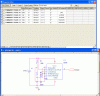
I am able to draw the schematic in Capture CIS and simulate it in PSPICE. I found some problem when I switch to the layout. The PCB footprint in the property editor in my attachment are left default. I have no idea what should be entered in the spread sheet if I'm using different package of IC or different size of the components. Is there any reference on this issue?
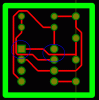
Besides, I opened Gerber tool from OrCAD layout and used auto rout. I found that the track is touching the pad and the DRC showed clean I wanted to edit the layout from the Gerber tool but I coundn't, I was able to move the track only. It is not as easy as eagle layout.
Any suggestion?
Thanks
I am very new to OrCAD and currently learning it. I'm using OrCAD 10.3.
I am able to draw the schematic in Capture CIS and simulate it in PSPICE. I found some problem when I switch to the layout. The PCB footprint in the property editor in my attachment are left default. I have no idea what should be entered in the spread sheet if I'm using different package of IC or different size of the components. Is there any reference on this issue?
Besides, I opened Gerber tool from OrCAD layout and used auto rout. I found that the track is touching the pad and the DRC showed clean
I wanted to edit the layout from the Gerber tool but I coundn't, I was able to move the track only. It is not as easy as eagle layout.Any suggestion?
Thanks