wuchy143
Member
I'm actually starting to learn the op-amp stuff and it appears a lot simpler than I remember. Granted, a couple of guys on here have significantly helped me grasp the concepts so it's clearly not that easy. That said...
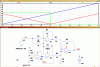
Ericgibbs gave me a circuit to try out. I've almost cracked the whole thing but I'm a little confused on the final op amp stage. (U6)
Some theory before I start math:
1. U8 is simply a buffer that has a voltage divider taking 14V and bringing it down to ~5V. This creates a nice output on U8 of +5V.
2. When Vin ramps up to >5V it makes U7 output go low. Which then allows U5 "+" pin to track Vin
Here are my calculations thus far:
U5:
k = gain_inverting = R1/R3 = 1k/1k = 1
Non-Inverting = 1 + k = 2
@V2 = 10
U5_Output = 2(5) - 0 = 10V (matches simulation)
U6:
I'm a little confused how to approach this guy. So far I know:
k = Gain_Inverting = R5/R6 = 1
Non_Inverting = 1 + k = 1 + 1 = 2
though I'm not very confident in these calculations....can anyone help me with this part of the circuit.
I attached my LTspice file and gave a screen shot of what I'm getting.
Attachments
Last edited:
")