Continue to Site

Welcome to our site!

Electro Tech is an online community (with over 170,000 members) who enjoy talking about and building electronic circuits, projects and gadgets. To participate you need to register. Registration is free. Click here to register now.

  • Welcome to our site! Electro Tech is an online community (with over 170,000 members) who enjoy talking about and building electronic circuits, projects and gadgets. To participate you need to register. Registration is free. Click here to register now.

Need help: Type II compensation/feedback

Status
Not open for further replies.

darkfeffy

New Member
Hi all,
I am trying to design and test a type II compensator for a synchronous boost converter. I obtained the control-to-output transfer function (credits to "Fundamentals of Power Electronics by R W Erickson") for the ideal case. The circuit parameters are:
Vin = 42V
Vout = 189V (approx 77% duty)
L = 1mH
C = 1000uF
Load = 4170VA
The PWM controller is the UC3823n with Vm = 1.8V (peak to peak).
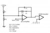
In order to eliminate the effect of the Right Hand plane zero and in order to move the cross-over frequency further, I designed a type 2 compensator (please see attached diagram) for a 5% overshoot and a < 0.1s settling time (on MATLAB).
The thing is IT DOESN'T WORK. Either the output is 44V or just erratic.
As I am not yet at under any serious load condition (large output impedance), could this be the cause of the poor operation of the control system? I replaced the UC3823n with a simple function generator and the boost gave 192Vdc with 77% duty (means my power-electronics setup is ok).
Can anyone suggest values for R3,C1,C2 for the compensator (as per the attached diagram)?
Regards
ed
 

Attachments

  • Type II compensation.JPG
    Type II compensation.JPG
    15.7 KB · Views: 1,406
You compensator is an integrator; there is no DC feedback around the opamp. It looks to me that you are building a PID feedback controller with only the I (integral) term. Seems like every time I tried to do this, I built an oscillator; not a damped output control system.

Seems like you need a P (proportional) term too.
 
Last edited:
Without doing the sums myself, the compesation you done looks 'about right' to me.

Only goes screwy closed loop?

Not something silly like the real X-over frequency too high (more than 5 kHz) is it? Maybe grounding or something?

You could try grossly over-compensating to get it stable in closed-loop, then work backwards?
 
That is in deed a type II compensation circuit.

Any reason you can't go to current mode control, eliminate the Right Half Plane Zero and use type I single pole compensation (simple integrator)? How exactly are you controling the synchronous "rectifier"?
 
Last edited:
That is in deed a type II compensation circuit.

Any reason you can't go to current mode control, eliminate the Right Half Plane Zero and use type I single pole compensation (simple integrator)? How exactly are you controling the synchronous "rectifier"?

Yes I was looking at the schematic on the other thread. I'm puzzled why it's not CM control, maybe there's no need for overload/core saturation /etc. protection.

I'm also even more curious why it's a synchronous rectifier design in the first place. They are more trouble than they are worth above a few volts. Sometimes they get into a product for marketing reasons, but it adversely affects MTBF, especially for aerospace stuff where conv efficiency is less important than reliability. Must be a good reason, I wonder why?
 
Last edited:
There are many things wrong...

A 1000µF cap rated for 198V???

22A of load current is why he wants synchronous.

The error amp is not connected

Max on time current ramp is ~8A... why 2 FET's?

That's just a quick look....
 
Last edited:
Thx for the suggestions. However, I would like to make a few points:

MikeMi
=====
It's a type II compensator I was trying to build. The Proportional term has a magnitude of 9.7dB (about 3.05 unitless). The trnsfr function of the compensator is 3.055 (1 + .0013s)/(1 - 0.00012s).

Marcbarker
========
I used synchronous rectification for two reasons:
(1) To avoid entering Discontinuous Conduction even in low load conditions. I am not very particularly fond of DCM because of the more complex equations involved.
(2) Fast discharge of capacitor (safety) and current bidirectionality. Could be useful in a motor application. But actually, I am intending to use this in some kind of UPS.
Normally, in full load, the anti-parallel diode of the sync rectifier will conduct. In low load conditions, the sync rectifier mosfet will conduct the inductor reverse current. I am using a Gate driver with bootstrap capacitor (for the floating sync rectifier). Forces me to use a NAND gate between the Pwm driver and the mosfet driver (so as to re-reverse the pulse signals).

Indulis
=====
I have a 1000uF,400V electrolytic capacitor. But the truth is its capacitance drops at high frequencies. At 10kHz, using an LC meter, it is less than 100uF. Guess at 50kHz, it should be lesser. So, I have paralleled it with a few ceramic capacitors just for purposes of reducing ESR (which I do not know exactly) and slightly increasing the capacitance.
I do not want to use current mode control for now because I want to avoid design complications (double loop in feedback). Also, given where I live, it will be difficult to find a Rsense resistor for a 100A rating (peak current in main switch).
I am thinking one reason for my problem is that I used the ideal Gvc (Control-to-Output) transfer function. I am currently trying to derive the Gvc taking into account the inductor series resistance, switch on-resistance, diode forward voltage and on-resistance.
But I am afraid I will be taking a shot in the dark. Someone help.
Regards
Ed
 
It's a type II compensator I was trying to build. The Proportional term has a magnitude of 9.7dB (about 3.05 unitless). The trnsfr function of the compensator is 3.055 (1 + .0013s)/(1 - 0.00012s).

The partial schematic you showed has the output of the "compensator" going to a PWM. If you were building a true PI controller, the P term would be summed with the I term BEFORE going to the PWM. I still see only an integral term.
 
The partial schematic you showed has the output of the "compensator" going to a PWM. If you were building a true PI controller, the P term would be summed with the I term BEFORE going to the PWM. I still see only an integral term.

After some verification, I think you are right. The Kp, Kd and Ki terms are supposed to be in parallel and summed up in the loop. I have referred to an application note and they keep calling it a PID controller though.
 
The partial schematic you showed has the output of the "compensator" going to a PWM. If you were building a true PI controller, the P term would be summed with the I term BEFORE going to the PWM. I still see only an integral term.
A Type II controller has just integral and differential terms and no proportional (DC) feedback. It will be stable with the proper compensation values. Leaving out the proportional term has the advantage of no DC steady-state error in the output voltage.

darkfeffy, did you do a small-signal, closed loop simulation of the system with a gain block simulating the PWM generator? I performed such a simulation for a Buck switching regulator I designed to optimize the feedback elements (which indicated some adjustment was needed from the calculated values for best stability), and the built circuit operated very close to the simulations. Can you post a block diagram of your simulation with the block transfer functions?
 
Last edited:
A Type II controller has just integral and differential terms and no proportional (DC) feedback. It will be stable with the proper compensation values. Leaving out the proportional term has the advantage of no DC steady-state error in the output voltage.

Ok, but I just went and looked at the OP's diagram again, and there is only a I term; nothing else...
 
Ok, but I just went and looked at the OP's diagram again, and there is only a I term; nothing else...
The diagram at the beginning of this thread shows a capacitor (integrator) feedback and RC (rate or differentiator) feedback, two terms.
 
How did you determine your values for the type 2? A synchronous makes no sense at 189V! Above 5V, they generally incur greater loss than non-synchronous. At this output level, a synchronous should not even be considered.

If the converter enters dcm at light loads, so what? All do. I use ccm, but at light loads, my type 2 comp is taylored to remain stable all the way to no load.

Your comp network has a zero at 128 Hz and a pole at 1,594 Hz. You have a low bandwidth for your servo loop. Your rhpz is at 1,516 Hz, less than your highest pole. This is unstable. The 0 dB crossing point should be 30% to 40% of the rhpz frequency.

Recruiting outside help is what I'd recommend. An SMPS is not rocket science, but not trivial either. Is this a project for a paying client? I'd look for a power electronics specialist or firm. THis requires someone who has been there and done that. BR.
 
Last edited:
Marcbarker
========
I used synchronous rectification for two reasons:
(1) To avoid entering Discontinuous Conduction even in low load conditions. I am not very particularly fond of DCM because of the more complex equations involved.
(2) Fast discharge of capacitor (safety) and current bidirectionality. Could be useful in a motor application. But actually, I am intending to use this in some kind of UPS.
Normally, in full load, the anti-parallel diode of the sync rectifier will conduct. In low load conditions, the sync rectifier mosfet will conduct the inductor reverse current. I am using a Gate driver with bootstrap capacitor (for the floating sync rectifier). Forces me to use a NAND gate between the Pwm driver and the mosfet driver (so as to re-reverse the pulse signals).
Maybe I'm missing something today, but how does having SR avoid DCM operation? Once the L stored energy is spent, I wouldn't of thought it made much difference what method of rectification.

Talking of loops, maybe (>50% DC?) you just only need to add a slope control or something? < I'm not sure about this, don't worry if it didn't make sense!

I have a good system for dealing with complex interpendent calculations. That is 'tune it by ear' with a scope and look at control loop waveforms! After all a circuit is an analogue computer. Then later do bodeplots to prove you have enough PM & GM. Then do the maths last! :D
 
Last edited:
...
darkfeffy, did you do a small-signal, closed loop simulation of the system with a gain block simulating the PWM generator? I performed such a simulation for a Buck switching regulator I designed to optimize the feedback elements (which indicated some adjustment was needed from the calculated values for best stability), and the built circuit operated very close to the simulations. Can you post a block diagram of your simulation with the block transfer functions?

Crutshow, here is the block diagram. Curiously enough, MATLAB has "difficulties" simulating (*step response*) when you put the compensator pole very close to the RHP zero (of the control-to-output tf).
Regards
 

Attachments

  • tf of boost.JPG
    tf of boost.JPG
    29.4 KB · Views: 601
Last edited:
...(1)How did you determine your values for the type 2?
(2) A synchronous makes no sense at 189V! Above 5V, they generally incur greater loss than non-synchronous. At this output level, a synchronous should not even be considered.

(3) If the converter enters dcm at light loads, so what? All do. I use ccm, but at light loads, my type 2 comp is taylored to remain stable all the way to no load.

(4) Your comp network has a zero at 128 Hz and a pole at 1,594 Hz. You have a low bandwidth for your servo loop. Your rhpz is at 1,516 Hz, less than your highest pole. This is unstable. The 0 dB crossing point should be 30% to 40% of the rhpz frequency.

(5) Recruiting outside help is what I'd recommend. An SMPS is not rocket science, but not trivial either. Is this a project for a paying client? I'd look for a power electronics specialist or firm. THis requires someone who has been there and done that. BR.

Claude,
(1) I determined the type II values using the attached pdf (somewhere near the end of the document).
(2) Both of my Mosfets have anti-parallel diodes. Meaning in normal high load conditions, this converter should function like an oridinary boost without sync. In low load (low currents), the Mosfet of the sync will conduct. So the losses are low (compared to the ordinary boost) and I don't think efficiency is a problem here.
(3) I wasn't sure if the PWM controller could operate all the way from CCM to DCM suddenly and rapidly. Why don't you tell me how you did it?
(4) Thx. I am rechecking my bode plots, compensator, etc...But a little confusion here. When you say "The 0 dB crossing point should be 30% to 40% of the rhpz frequency", are you talking of the compensator (Gc) alone or of the whole system compensated (Gc * Gvd / Vm ) with feedback?
(5) Would be greatful if u could show me how u did it...
Merci (that's french)
Edwin
 

Attachments

  • Topic_3_Lynch.pdf
    1.9 MB · Views: 440
Maybe I'm missing something today, but how does having SR avoid DCM operation? Once the L stored energy is spent, I wouldn't of thought it made much difference what method of rectification.

Talking of loops, maybe (>50% DC?) you just only need to add a slope control or something? < I'm not sure about this, don't worry if it didn't make sense!

I have a good system for dealing with complex interpendent calculations. That is 'tune it by ear' with a scope and look at control loop waveforms! After all a circuit is an analogue computer. Then later do bodeplots to prove you have enough PM & GM. Then do the maths last! :D

Marcbarker,
I read an interesting explanation about DCM that said one can look at things from a conservation-of-energy point of view. The inductor current cannot go to zero instantaneously (spelt that right?). If this were so, this would need phenomenal amounts of energy. Now, in a classical boost, the diode which is unidirectional is the main truand here. Since we must conserve energy, the reverse current (which is not allowed to flow) will "express itself" by causing the voltage at the output to rise...
I find that explanation pretty "crude" and "intiutive".
About "tune it by ear", do you mean trying different values of R and C and observing the error reduce progressively? I thought of this but i got frightened :D. I might be shooting in the dark. At one time, my gate driver got bad after the erratic behaviour of the control system.
Regards
 
I believe the gain of you PWM block is much too low. If 77% duty-cycle gives 192V then 100% duty-cycle would give 250V. The PWM gain should thus be 250/1.8, not 1/1.8. That extra loop gain could be causing your instability. Try recalculating the compensation values and resimulating with the higher PWM gain.
 
Last edited:
Status
Not open for further replies.

Latest threads

New Articles From Microcontroller Tips

Back
Top