Continue to Site

Welcome to our site!

Electro Tech is an online community (with over 170,000 members) who enjoy talking about and building electronic circuits, projects and gadgets. To participate you need to register. Registration is free. Click here to register now.

  • Welcome to our site! Electro Tech is an online community (with over 170,000 members) who enjoy talking about and building electronic circuits, projects and gadgets. To participate you need to register. Registration is free. Click here to register now.

Need help: Type II compensation/feedback

Status
Not open for further replies.
Marcbarker,
I read an interesting explanation about DCM that said one can look at things from a conservation-of-energy point of view. The inductor current cannot go to zero instantaneously (spelt that right?). If this were so, this would need phenomenal amounts of energy. Now, in a classical boost, the diode which is unidirectional is the main truand here. Since we must conserve energy, the reverse current (which is not allowed to flow) will "express itself" by causing the voltage at the output to rise...
I find that explanation pretty "crude" and "intiutive".

Or another way I like to analogise it, the inductor is a 'flywheel' for current. When current gets pushed into it, the flywheel spins up and gains momentum. The momentum as the flywheel spinning down is the energy stored. While spinning, if an attempt is made to impede that flywheel current (i.e. a switch is 'mode-ed'), the inductor will make whatever voltage is neccessary to maintain that same current. When you're 'thinking currents' (instead of voltage), imagine the current has momentum.

About "tune it by ear", do you mean trying different values of R and C and observing the error reduce progressively? I thought of this but i got frightened :D. I might be shooting in the dark. At one time, my gate driver got bad after the erratic behaviour of the control system.
Regards
Yes, an educated empirical approach, can do a bode plot with real hardware, and scope the shape of control waveforms. I was lucky to had been taught very early in my career some neat tricks with tuning control loops, by some older people who knew lots of short cuts. Looking at the shape of a control loop closely (not just the shape 'critically damped') you can tell a lot, rather like Smith Charts are to RF analysis :) It's probably better the way you are doing it though, mathematically, but something I've noticed about entire mathematical solutions is that at the end of a load of sums that fail acid test, an elusive little mistake crept in somewhere, it's hiding in a corner!
 
Last edited:
No, you have 4170VA (load) with an output of 189V that's ~22.06A

It would be impossible to get 100A through a 100µH inductor at 50KHz with 48Vin!!!
(E*t)/L=i


Punch the #'s in for yourself:

Switching Converter Power Supply Calculator

Have a look at the jpg.
Pk current = Iav + I ripple
If ripple is small (say less than 5%) then Pkcurrent =~ Iav = Iinductor.
The ramp is the current thru the inductor. The red-shaded area is the current thru the main switch. The green-shaded is the current thru the diode(sync rect). ALL have the same Peak current. What u calculated(22A) is the rms current through the load (i.e thru the diode (or sync rectifier)). If not convinced take a look at fundamentals of power electronics by RW Erickson.
But we are straying from the point here. My problem is control. Please, any help you can provide will be highly appreciated.
regards
 

Attachments

  • boost.JPG
    boost.JPG
    30.5 KB · Views: 206
Hi darkfeffy,


Are you sure all the info you provided is correct? The reason i ask is because
your flow graph comp network equation looks like it is missing something, and
your other equation looks like it has a rather large constant term. So, how
did you come up with the equation for your plant? Also, is there a complete
circuit we can have a look at? And how did you get only a first power of 's'
in your compensator equation when there are two active elements in it
in the schematic?
This is very important because if we get the
wrong information we can never offer a good suggestion.
Right now it looks as if your plant is not controllable, but if you are working with
a relatively common circuit then my guess would be that the equation was
not extracted correctly.
 
Last edited:
The inductor should be in 10 to 12 uH range. Stability analysis should include Rs of devices, filter cap, and saturation characteristics of inductor. The inductance will drop at the full current. Coil winding and core design should not let inductance drop more then 20-25%. Usually want to keep loop bandwidth up as high as possible to get good transient load response. Like 1 Khz.

You are not likely to accomplish this with a single coil.

This power supply is very similar to what is used in DC to AC inverters where 12v-48v battery is pumped up to 155 vdc for modified sinewave inverters or 185 vdc for PWM sinewave inverters. In these cases the boost circuit uses a push-pull primary with separate HV secondary for isolation. For something like a 4kW inverter multiple parallel transformers and switchers are used.

Also pushing to 50 KHz switching with this output is going to be tough for the rectifiers. Got to use ultra-fast 500-600 piv.

I would not recommend bitting off a 4kW switcher as a first project. Try a scaled down version in 100-300 watt range. Less sparks will fly on any mistakes.
 
Last edited:
Attached is a very old schematic for a modified sinewave inverter.

It is like 30 years old before there was neat MOSFET bridge driver I.C.'s

It will give you a general ideal on the D.C. boost supply at the top of the schematic. The ferrite transformer for the 300 watt supply is about 2 inches square. I think it was operating at 25 kHz.
 

Attachments

  • Power Inverter Schematic.pdf
    135.5 KB · Views: 940
Hi darkfeffy,


Are you sure all the info you provided is correct? The reason i ask is because
your flow graph comp network equation looks like it is missing something, and
your other equation looks like it has a rather large constant term. So, how
did you come up with the equation for your plant? Also, is there a complete
circuit we can have a look at? And how did you get only a first power of 's'
in your compensator equation when there are two active elements in it
in the schematic?
This is very important because if we get the
wrong information we can never offer a good suggestion.
Right now it looks as if your plant is not controllable, but if you are working with
a relatively common circuit then my guess would be that the equation was
not extracted correctly.

Hi MrAI,
Here is how I came up with the compensator.

1. I calculated the control-to-output transfer function for the ideal boost converter. Using section 8.2.2 of “Fund of Pwr Electronics” with the following parameters:
Vin = 42V; Vout = 189V; Power = 4170VA; L = 1mH; C = 1000uF.
I obtained Gvd (please see picture 1 – I do not know how to insert a photo directly in the text).

2. Obtained the transfer function of the duty cycler. Simply used 1/Vm where Vm is the valley-to-peak voltage of the ramp. The UC3823n has Vm = 1.8V.

3. Obtained the feedback gain H(s) as 1/74. Voltage divider circuit which should give 2.55V when output is 189V.

4. For now, I used no compensator i.e. Gc(s) = 1.

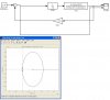
5. Plotted the root locus of the uncompensated system with these parameters (please see picture 2). As expected, there is a RHP zero at 1.3kHz and two complex LHP poles at 35Hz. The system is UNSTABLE (because there are loci in the RHP).

6. I set the design objectives as: Settling time < 0.05s; overshoot < 5%.

7. Compensator design starts:
a. Inserted a pole very near the RHP zero. This has the effect of cancelling the loci in the RHP. I chose a RHP pole at 1.326 kHz.
b. Inserted a zero in the LHP. This has the effect of “pulling” the root locus towards the left. I chose a LHP zero at 122 Hz.
c. As of now both these actions result in a compensator with a unity gain.
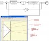
d. Noticing that the closed-loop poles were not really satisfying the design objectives (settling time and overshoot), I moved them till they satisfied these objectives. This gave a gain of 3.055 (i.e. 9.7dB).
e. Please see picture 3 for the overall compensated system showing the design objectives.

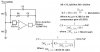
8. Using a note from Texas Instruments (I posted it earlier in this thread. It is called “Topic 3”), I designed the compensator components as shown in picture 4.

I wish to add that unlike what RCinFLA thinks, I am not testing at 4kW yet. I am using a much reduced model. In fact during testing, the ONLY load was the voltage divider at the output. I was thinking that if the control system works for a little model, it should perform as well for a larger model (if working with the same circuit params). I also want to master the design of such control systems so as to modify circuit parameters and still obtain desired results.
Please point out all errors I made (this is certain because the control system did not work) and suggest a methodology. Thanks for your useful suggestions and remarks.
Edwin
 

Attachments

  • Picture 1 - Gvd Transfer function.JPG
    Picture 1 - Gvd Transfer function.JPG
    7.8 KB · Views: 180
  • picture 2 - tf of boost uncompensated.JPG
    picture 2 - tf of boost uncompensated.JPG
    68.8 KB · Views: 224
  • picture 3 - tf of boost compensated.JPG
    picture 3 - tf of boost compensated.JPG
    80.8 KB · Views: 256
  • picture 4 - compensator elements.JPG
    picture 4 - compensator elements.JPG
    36 KB · Views: 271
Attached is a very old schematic for a modified sinewave inverter.

It is like 30 years old before there was neat MOSFET bridge driver I.C.'s

It will give you a general ideal on the D.C. boost supply at the top of the schematic. The ferrite transformer for the 300 watt supply is about 2 inches square. I think it was operating at 25 kHz.

Hi RCinFLA,
Thanks for the suggestions and the link. Concerning the link, I examined the diagram. In effect, the boost part is a push pull configuration at about 25kHz (Rt,Ct combination yields this frequency).
Tried reverse-working the compensator frequencies from the values of the feedback compensator elements. Seems that the compensator pole frequency f_p is at 0 while the zero frequency f_z frequency (fz) is 1.592kHz with a gain of -32.869dB (corresponds to 0.023). Seems "my" gain is far above this. How did they obtain this value?
Is push-pull absolutely necessary for this project? I ask because my pwm controller UC3823n is not push pull. And too, I want to avoid a transformer if possible. I am not working at 4kW yet... I am still almost off-load with a reduced model.
Thx. Edwin
 
2. Obtained the transfer function of the duty cycler. Simply used 1/Vm where Vm is the valley-to-peak voltage of the ramp. The UC3823n has Vm = 1.8V.
As I previously noted, your duty cycler gain is much too low. You did not include the gain from the duty cycler output to the switch output. 0 to 100% duty-cycle gives 0 to 250V output. Thus the gain from the duty cycler input to the switch output is 250/1.8 not 1/1.8. The high gain factor of 250 times what you used likely will cause instability if not accounted for in your compensation network.
 
As I previously noted, your duty cycler gain is much too low. You did not include the gain from the duty cycler output to the switch output. 0 to 100% duty-cycle gives 0 to 250V output. Thus the gain from the duty cycler input to the switch output is 250/1.8 not 1/1.8. The high gain factor of 250 times what you used likely will cause instability if not accounted for in your compensation network.

For the ideal boost, 100% duty should give an infinite output voltage. For the real boost, 100% duty should give 0V. The relationship b/w input & output is non-linear (vout = vin/(1-D)).
Regards
 
Hi again,


Well, i asked to see your plant because i have no trouble compensating a
normal buck output circuit but you seem to be having a problem here, so
i thought maybe there was something wrong with the equation for the plant.
If you show me that i might be able to help more, but without that i can
only take a guess (see below).
I ask about this because there are a couple of problems, as i said:
1. Your compensation equation only shows one power of s, yet the scheme has
two capacitors. Are you considering one to be insignificant?
2. Your compensator equation part looks like this:
3.055*[0.0013 1]
and there is a space between the '13' and the last '1', what does that mean?
That space makes no sense so you should explain that.

In the mean time here is a guess on what to try:

C1=10uf (with + terminal toward op amp input)
C2=100pf
R3=1k
Across R1 a forward network:
1k in series with 0.15uf cap
Across R2:
4.7v zener, anode to ground.

Try these and report back.
 
Last edited:
For the ideal boost, 100% duty should give an infinite output voltage. For the real boost, 100% duty should give 0V. The relationship b/w input & output is non-linear (vout = vin/(1-D)).
Regards
I did a buck regulator, which has a linear relationship between duty-cycle and output voltage, and I forgot that the transfer function for a boost regular is a non-linear function.

But the point is that the vin/(1-d) relationship needs to be in your loop simulation, and it isn't.
 
Also, in continuous mode the RHPZ moves with load and line (if you want a real headache, throw in temperature variation). For it to be stable the crossover frequency will be very low so the transient response won't be "great".
 
Last edited:
Hello again,


With this changes:

C1=10uf (with + terminal toward op amp input)
C2=100pf
R3=1k
Across R1 a forward network:
1k in series with 0.15uf cap
Across R2:
4.7v zener, anode to ground.

I was using all of his input information about the plant and the other
variables. I would prefer to see the whole circuit so i can make my
own judgments on how best to model a given part of the circuit, so
i am hoping he shows us more of the original design. I dont know how
private his design has to be though, but heck how different can it really
be from the million other buck regulators out there :)
Keeping that in mind, the above changes produce a fairly quick response
that exceeds his requirements.

Hi MrAI,
Thanks for your suggestions.
I appologise for my assumptions. Actually, in MATLAB [a b] for a transfer function means aS + b. Similarly, [a b c] would mean aS^2 + bS + c... and so on. MATLAB represents transfer functions as row matrices.
I am grateful for your suggestions on compensator values. Immediately I get to the lab, I'll try them and give feedback as you said. Then (when it works) you owe me a COMPREHENSIVE course on compensation.:)
I will post my boost design if that is necessary (didnt think so given that it is a classical boost structure but with a sync rectifier - and which worked when I used a function generator instead of the pwm controller). Right now I am on the move, in about 4 hours time, i'll post the design.
Regards
Edwin
 
Also, in continuous mode the RHPZ moves with load and line (if you want a real headache, throw in temperature variation). For it to be stable the crossover frequency will be very low so the transient response won't be "great".

Hi Indulis
I am hoping to get something working soon.
Unless the transient response is going to damage my equipment and components, I don't really care about it right now. I just want steady state to remain at 189Vdc.
Thanks
Edwin
 
Status
Not open for further replies.

Latest threads

New Articles From Microcontroller Tips

Back
Top