Hi All!,
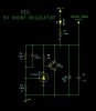
I'm trying to figure out how this 5V shunt regulator works and am just confusing myself. I attached a schematic to avoid confusion.
I see that R4 and U1 are where the engergy is shunted to but as for how the PNP dumps this energy there to be dissipated is confusing. Does anyone have a simple explanation at to what's going on here? I know it's not too complicated....
Thanks!
-mike
Look at the attached simplified equivalent circuit taken from the LM431 data sheet. Note that if Ref (+ input of the opamp) is a mV or so HIGHER than the 2.5V reference, the gain of the opamp drives the built-in NPN into conduction, pulling the Cathode voltage down toward the Anode.
If Ref is a mV or so LOWER than 2.5V, then the NPN is off, meaning that the external circuit can pull the Cathode up as high as it can (no current flows through the collector of the NPN).
Note that in your circuit, the Ref input is driven by a voltage divider consisting of two equal value resistors (1% no less), so that sets the regulation voltage at twice the internal 2.5V reference, i. e. 5V.
Also notice that if the output of the regulator is slightly higher than 5V, that makes the Ref input slightly more than 2.5V, which causes the LM431 to sink current out of the base of the power PNP TIP34 transistor, which gets amplified by the β of the transistor, which causes a much larger current to flow from the output node to ground via the collector of the transistor.
The transistor current adds to the current flowing in R1 (1Ω resistor), which increases the drop across R1 in an amount such that the voltage at the output stays at 5V.
Another way to think of this is to suppose that the external load on the power supply was suddenly cut in half. The reduction in current would naturally cause the output voltage to rise. However, the TL/LM431 sees the increase in output voltage and reacts by turning on the TIP34 harder. This "shunts" current to ground exactly offsetting the reduction in load current keeping the drop across R1 (and the output voltage) constant.