Continue to Site

Welcome to our site!

Electro Tech is an online community (with over 170,000 members) who enjoy talking about and building electronic circuits, projects and gadgets. To participate you need to register. Registration is free. Click here to register now.

  • Welcome to our site! Electro Tech is an online community (with over 170,000 members) who enjoy talking about and building electronic circuits, projects and gadgets. To participate you need to register. Registration is free. Click here to register now.

Multistage BJT amplifier

Status
Not open for further replies.

Fluffyboii

Active Member
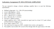
Hi, fist of all I want to say that I am unable to understand how BJTs operate. It seems simple, I calculate the values but when I try to simulate it on LTSpice or test it in real life things start to not make sense. When we started using Op Amps in class I was overjoyed because those thing act as they should in calculations because they are designed for it. But now they want us to make a multistage BJT amplifier with almost no information and just the requirements.

The hardest part seems to be achieving input impedance over 1M ohms. Also when I look at 2n2222 datasheet it says the Beta value is 35 but when I put one of those in my transistor tester I see values over 400. BC547 or similar BJTs show again higher than 300 Hfe values which makes no sense.

Anyway for my first test I decided to use a common emitter setup with high Re value to get a high input resistance. From my book it says the input resistance of a BJT CE amplifier is (B+1) (re +Re) so if I pick Re something like 3K ohms I should have over 1.2M ohm input resistance which is what I exactly did. The general rule of thumb seems to have %10 of voltage supply as voltage drop on Re so I picked 1.5V (15V supply) +0.7V should give me 2.2V Vb. Set the bias with a voltage divider. For my Ic value I picked 0.5mA and that gave me 15K ohm Rc resistance for 7.5V voltage drop on Rc. At the end I should have around -15K/3K = -5 times gain right? I assumed Ic and Ie as same since BJT has over 400 Beta.

Ok this was correct. I was having a delusional nightmare when I saw 8V and assumed 800 times gain but when I remember 7.5V center and saw 8V max and 7V bottom voltages I realised it was correct. Sometimes ranting about how stupid something makes me realise how stupid I am.

What can I do to have less than 100 ohms output resistance. I obviously need to increase the gain first. Logical thing to do seems to add a 20 times gain CE amplifier series with the first one to get non inverting 100 times gain then buffer it with another BJT to decrease the output impedance. But adding transistors in series causes them to affect each other and I am not sure how to pick the values for the second stage without distorting the signal. And how do I design them to have 20 times gain. I start with Ic current than calculate the other values from there which makes it hard to get the wanted gain without trial and error. I am sure there is a easy way to manipulate the equations and find it but I am unable to think right now. Actually it looks like If I pick Rc and Re values low enough I may be able to get away with only 2 stages without additional buffering.
 

Attachments

  • Screenshot_5.png
    Screenshot_5.png
    177 KB · Views: 202
  • Amplifier.asc
    1.2 KB · Views: 209
Transistors are current amplifiers; that's the essence of what you need to know. Most other parts come down to Ohm's Law.

eg. This is a basic single transistor amplifier stage, found all over the internet, that can be cascaded for more gain; the output cap becomes the input cap of the next stage.

B5F_Fig_1.jpg


The way I go about designing with that circuit is firstly decide the standing bias current, probably 10 - 20mA for a general purpose amp stage.

You know the intended supply voltage.

Then calculate Rc to drop somewhere between a third and a half supply voltage at that current.

Set the DC gain (or only gain) by dividing Rc by the required gain, to get Re.

R1 and R2 then form a voltage divider to set the voltage on the base, which in turn sets the voltage on the emitter; that voltage should be calculated to set the original bias current in the emitter resistor.

The transistor base current will be the emitter current divided by its gain. The current in R1 & R2 needs to be either several times that so it does not affect the voltage too much, or you need to reduce the upper resistor slightly to allow for the base current.

You can think of the bias voltage and emitter resistor rather like a typical, simple, constant current circuit -
Except, variations in the vase voltage also vary the emitter voltage (like an emitter follower circuit) and so modulate the emitter and collector current...

The variations in collector current cause a much larger variation across the collector load resistor, giving amplification of the input signal.

Adding Ce (or a capacitor in series with a resistor) across Re mean the AC signal gain will be higher, by the ratio of the overall emitter load impedance at whatever the signal frequency is.


eg. A rough example:
15V supply, 10mA standing current.
Collector voltage around 9V, so 6V across Rc; 600 Ohms. Use 560.

Gain of 10, so emitter 56 Ohm; and 0.6V across that with the same current as the collector.
That means bias around 1.2 - 1.3V as a starting point.

Rough estimate bias chain eg. 200uA to be several times base current; that means somewhere around 75K total.
15 (total volts) / 1.3 (target bias) = ~11.5
75 / 11.5 = 6.5, call it 6.8K

75 - 6.8 = 68.2, so the upper resistor can be 68K and the lower 6.8K

That gives a starting point, adjust as needed to get a sensible collector voltage with roughly equal readings across the collector resistor and transistor.


That would likely do as the second stage of the amp, with a similar one but all resistors eg. 5 * higher values as the first stage?

That should give gain of around 100 and non-inverting (via double inversion) as required.

Then you need to add a buffer stage to provide the low output impedance.
 
Buffer part decreases the voltage for some reason. Tested with different values but couldn't get it going right, any ideas why?
 

Attachments

  • Amplifier.asc
    2.5 KB · Views: 184
Last edited:
You have a 7.5K as collector load in the middle stage, then two 10K (so effectively 5K) as bias for the buffer.
In most cases, the input impedance of any stage should be a lot! higher than the output of the one driving it, to avoid attenuation and distortion.

I've tweaked the values and adjusted the gain a bit to get the required response and levels, into the 100 Ohm load as stated.

You need to add an input buffer to get the input impedance above 1 Mohm as in the requirements..
 

Attachments

  • Amplifier_test.asc
    3.1 KB · Views: 177
You have a 7.5K as collector load in the middle stage, then two 10K (so effectively 5K) as bias for the buffer.
In most cases, the input impedance of any stage should be a lot! higher than the output of the one driving it, to avoid attenuation and distortion.

I've tweaked the values and adjusted the gain a bit to get the required response and levels, into the 100 Ohm load as stated.

You need to add an input buffer to get the input impedance above 1 Mohm as in the requirements..
I see that you decreased 7.5K to 1K and adjusted accordingly and also increased buffer input resistance. But why did you decrease the Collector resistance of the second stage. If the input impedance of the stage needs to be lot higher than the output of the one driving it I would expect to use a higher Rc and Re value for the middle stage. For the input buffer I need to use lot higher value resistors for biasing I assume. One final thing: Do I need the emitter bypass capacitor at the fist amplifying stage. I understand that it increases the gain but I wonder if the same effect couldn't be achieved with lower Re value.
 
But why did you decrease the Collector resistance of the second stage. If the input impedance of the stage needs to be lot higher than the output of the one driving it I would expect to use a higher Rc and Re value for the middle stage.

The third stage has a 10K bias resistor to positive, plus (I can't remember what) to negative, which can be considered in parallel as far as input impedance goes.

The driver output impedance needs to be a lot lower to minimise attenuation and distortion, which the 1K collector load in the second stage is.

I usually prefer to avoid the emitter bypass cap, but going too low with just an emitter resistor makes the biasing very critical, as the emitter steady state voltage is so low. A higher value Re plus a capacitor-resistor bypass makes it less critical while providing controlled gain.


The commonest audio gear I know of that uses inputs in the 500K - 1M range is guitar gear. I've never seen a bootstrapped one, but many different emitter follower buffers; eg.


I added an input buffer as you suggested. Biased it as recommended in the link you sent. Since transistors I use have around 400 Beta input impedance should be over 1M with 2.5K emitter resistor I think.
 

Attachments

  • Amplifier_test2.asc
    3.7 KB · Views: 185
Two, 50K bias resistor in parallel means 25K impedance at that point, before you even get to the transistor.
That is the "Thevenin equivalent" of the two bias resistors.

As long as the buffer transistor has a gain of over 400, its input impedance should be over one Megohm. The emitter resistor could be made a bit higher, eg. 4k7, to give a better margin.

I've modified the bias circuit to separate the voltage divider from the transistor base, using a separate base resistor. That 1M is adding loading to the input making the input impedance less than 1M overall, so I've also added a bootstrap cap as Nigel suggested, to minimise the loading caused by that resistor.


Thinking further, it should be possible to use a higher value still in the emitter, eg. 10K, and directly connect the base of the next transistor to that, eliminating it's coupling cap and bias resistors, just setting the bias of the buffer to give the same voltage at the buffer emitter as the second stage base has at present.

That would further increase the input impedance of the overall circuit.
 

Attachments

  • Amplifier_test_2.asc
    4.3 KB · Views: 174
Two, 50K bias resistor in parallel means 25K impedance at that point, before you even get to the transistor.
That is the "Thevenin equivalent" of the two bias resistors.
My idea was to just increase them until it satisfies the req but using a voltage divider for biasing in that case is probably not the best idea, thanks for helping will report back after building the circuit.
 
rjenkinsgb
The circuit worked as intended, only problem I had was measuring input and output impedances. The input impedance seem to be something infinite. Also 100 ohm resistor at the output buffer caused some distortions but switching it with 220 ohm one fixed the issue at the cost of low output impedance. Anyway assistants were ok with it at the end, thanks for fixing the circuit.
How are you measuring the impedances?.
 
How are you measuring the impedances?.
Adding a resistor between the source and the amplifier than finding the ratio of the new gain and old gain and similarly doing the same for the output.
The 1M resistor plus bootstrap should make it appear extremely! high.

The output distortion may have just needed a slight bias adjustment to optimise the working signal range, or the input was a bit high?
Input I used for testing was 50mV. I wish I tried changing the bias but I think 100Ohm output impedance requirement was a bit to low anyway it was heating up the emitter resistor to much. Actually in LTSpice it is supposed to pull more current (Re) but in real life it does not and causes the weird distortion when Re is 100 instead of 200 which causes the waves to look thicker and compressed.
 
I see so it doesn't scale like I thought it would.
Well there's little point altering the value of R2, as the whole idea of bootstrapping is to effectively make R2 very high impedance. It also has to be a low enough value to provide sufficient DC current to the base of the transistor.
 
Status
Not open for further replies.

Latest threads

New Articles From Microcontroller Tips

Back
Top