Continue to Site

Welcome to our site!

Electro Tech is an online community (with over 170,000 members) who enjoy talking about and building electronic circuits, projects and gadgets. To participate you need to register. Registration is free. Click here to register now.

  • Welcome to our site! Electro Tech is an online community (with over 170,000 members) who enjoy talking about and building electronic circuits, projects and gadgets. To participate you need to register. Registration is free. Click here to register now.

MOSFET STD85N3LH5 Bipolar Totem-pole Driver Circuit

Status
Not open for further replies.

KC23

New Member
Hi, I am a complete beginner in using MOSFET, so please bear with me.

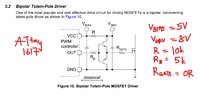
As attached is my schematic. I am using ATtiny1617 as my IC which outputs a PWM signal around 200Hz.
I am trying to turn on and off the gate of my N-channel MOSFET STD85N3LH5 using the totem-pole configuration.

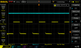
I have attached my signal as well.
CH1 yellow - Gate signal
CH2 blue - Vdrive

My issues:
1) I am expecting to get a 8V PWM on the gate signal but I am getting 5V instead. Is there something wrong with my understanding? Since I am supplying 8V to my VDRV.
2) The gate signal is not completely turned off, there is a slight delay as you can see from the waveform. Is it because of my PNP transistor selection?

Please kindly assist me.
Thank you.
 

Attachments

  • Screenshot 2021-10-08 120359.jpg
    Screenshot 2021-10-08 120359.jpg
    112.4 KB · Views: 265
  • DS1Z_QucikPrint1.png
    DS1Z_QucikPrint1.png
    39.4 KB · Views: 237
A transistor connected as an emitter follower has no voltage gain; in fact in that configuration, you lose about 0.6 - 0.7V from both the maximum and minimum voltages.

To get operation "outside" the MCU supply, add another NPN transistor or small FET between the MCU and driver; base (via resistor) or gate driven from the MCU and the collector or drain having a pull-up resistor to the higher voltage supply.

Adding a moderate value resistor between the bases and emitters of the power driver circuit will allow the output to have full range, but without any current boost for the highers & lowers 0.7V.

ps. I'd consider that driver config a "Class B" amplifier, not a totem pole.
 
I don't recognize your image source, but it contradicts the general wisdom of interface a uC to a FET but may be true for an open collector comparator with a pullup resistor and thus high impedance source. In the previous century, when CMOS 1st came out with 4xxx series devices the output impedance was generally high to prevent shootthru power dissipation thus ~ 1k @ 5V and ~ 300 ohms at 15V. So look at the emitter-follow (current amplifier) as an impedance reducer so output impedance of the emitter is Rout = Rin/ hFE , so if hFE =100 and Rin= 5k then Rout = 50 Ohms. But modern CMOS today has RdsOn of ~ 50 Ohms +/-25% typ. @ 5V and 74ALVxx CMOS like ARM's is rated for 3.6V and half the resistance of 74HCxxx family .

So the bottom line is that not only does it not help drive the FET due to the voltage drop of 0.7V , but it hurt the control of RdsOn of the FET by reducing the gate voltage called Vt or Vgs(th). This can range from 2 to 4V for older styles or higher voltage FETs or be <=1V for the "logic Level" type FETS which makes the transistors useless here as these were not available 40 yrs ago when your schematic image was probably created.

Conclusion: Consider that a history lesson and choose Logic Level FETs rated for at least 5x to 10x the current you intend to use and the Vdd you are using. if you want it cool. They usually specify RdsOn at -10% of common supply voltages. It is never used as a switch at Vgs(th) because that is just the threshold where it might conduct only 100 uA.

However your FET is only 5 mOhms and has a reverse capacitance of 58 pF typ. (Miller C) which means you can get glitches on the Vgs from flyback on the drain feedback. Often in half-bridge designs to prevent shoot thru, you must control Turn off faster than turn-on so diode R combinations. But a transistor could be used in this interface.

More specs are needed to choose the best topology.
 
Last edited:
What is your load voltage , current , impedance, & interface cable? These are important variables.

To boost Vgs one can use a common emitter with slower risetime from 1k than off time then Rce is < 10 ohms and input is say 3 to 6V for "1"

1633716545636.png
 
Last edited:
There is an asymmetrical driver impedance with the NPN CE switch which affects turn on/off slew rate if that matters. ON = 2 to 20 Ohms , OFF = Rc pullup . The 1k across Vbe is redundant and only when output source is disconnected or initialized as an input after power up. to disable drive.

By reducing R pullup for faster turn-on time as Ciss = 1.85 nF and Rc= 1k makes RC=T= 1.85 us and increasing Rbase reduces ON resistance and raises Vol.

Alternatively for much faster CE to complementary CC.
 
Last edited:
Status
Not open for further replies.

Latest threads

New Articles From Microcontroller Tips

Back
Top