I recently wasted 2/3rds of a circuit board and the last third barely passed in quality.
The first attempt failed with some traces missing but I could guess because the T5 insect killing lights haven't warmed up yet. I exposed it for 5 minutes and then developed for about one minute using a plastic container of 1 part of local sodium hydroxide (aka MGchemicals "developer") mixed with 10 parts water.
The second attempt also failed the same way but with traces missing in other places. The only thing I did different this time was increase exposure time to 11 minutes.
Now for the third attempt, I exposed for 5 minutes then this time, I developed for about one minute using a plastic container of 1 part of sodium silicate (DP-50 developer from Kinsten) and 4 parts of water. Yes I followed their directions. The board looked decent in the solution. So I took it out and after etching, it seems the traces were legible yet instead of pure dark tracks, I get them grainy, meaning there are thousands of little dots (like spots the same color as that of a circuit board without the copper layer) inside the traces.
In all three tests, I did the following:
1. For the artwork, I went to a local print shop to print the art dark with a professional lazer printer on a sheet of transparency and the image comes out very dark.
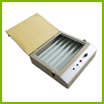
2. For exposing, I used this UV exposure unit. I had the knob turned all the way to the right in all tests.

Details of that unit are found here: **broken link removed**
Things were working better before the lights that came with the unit eventually burned out. Sadly there were no labels to the original lights so I ended up researching and ended up buying UV lights from the UK.
The listing is located here: http://www.ebay.ca/itm/6x-8W-T5-Ult...nsect-Fly-Killer-Mosquito-Zapper/322199166926
I replaced every light with the ones from ebay before running all three tests.
I think I read somewhere the 368 in the model number 368BL means 368nm which is between 350 and 400nm (the range for PCB presensitized layer). So the only thing that comes to my mind is that I should probably warm up the unit first with no board for 5 minutes, then after expose my board for 2 1/2 minutes only since I'm using light in the PCB layer range and probably the lights that were originally included in the unit were of higher wavelength?
or is 2 1/2 minutes still too long?
I'm a bit confused, but I don't want to have the developer strip away the good tracks.
The first attempt failed with some traces missing but I could guess because the T5 insect killing lights haven't warmed up yet. I exposed it for 5 minutes and then developed for about one minute using a plastic container of 1 part of local sodium hydroxide (aka MGchemicals "developer") mixed with 10 parts water.
The second attempt also failed the same way but with traces missing in other places. The only thing I did different this time was increase exposure time to 11 minutes.
Now for the third attempt, I exposed for 5 minutes then this time, I developed for about one minute using a plastic container of 1 part of sodium silicate (DP-50 developer from Kinsten) and 4 parts of water. Yes I followed their directions. The board looked decent in the solution. So I took it out and after etching, it seems the traces were legible yet instead of pure dark tracks, I get them grainy, meaning there are thousands of little dots (like spots the same color as that of a circuit board without the copper layer) inside the traces.
In all three tests, I did the following:
1. For the artwork, I went to a local print shop to print the art dark with a professional lazer printer on a sheet of transparency and the image comes out very dark.
2. For exposing, I used this UV exposure unit. I had the knob turned all the way to the right in all tests.

Details of that unit are found here: **broken link removed**
Things were working better before the lights that came with the unit eventually burned out. Sadly there were no labels to the original lights so I ended up researching and ended up buying UV lights from the UK.
The listing is located here: http://www.ebay.ca/itm/6x-8W-T5-Ult...nsect-Fly-Killer-Mosquito-Zapper/322199166926
I replaced every light with the ones from ebay before running all three tests.
I think I read somewhere the 368 in the model number 368BL means 368nm which is between 350 and 400nm (the range for PCB presensitized layer). So the only thing that comes to my mind is that I should probably warm up the unit first with no board for 5 minutes, then after expose my board for 2 1/2 minutes only since I'm using light in the PCB layer range and probably the lights that were originally included in the unit were of higher wavelength?
or is 2 1/2 minutes still too long?
I'm a bit confused, but I don't want to have the developer strip away the good tracks.
