Continue to Site

Welcome to our site!

Electro Tech is an online community (with over 170,000 members) who enjoy talking about and building electronic circuits, projects and gadgets. To participate you need to register. Registration is free. Click here to register now.

  • Welcome to our site! Electro Tech is an online community (with over 170,000 members) who enjoy talking about and building electronic circuits, projects and gadgets. To participate you need to register. Registration is free. Click here to register now.

Low-Power AM Broadcast Band Transmitter

Status
Not open for further replies.

VA6GDG

New Member
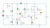
I'm building the attached low-power AM Broadcast Band Transmitter by Andy Collinson (left-most image - amtx.gif). It's to help out a few young fellows with their interest in radio.

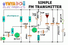
I notice that the circuit is VERY similar to many of the low-power FM Transmitter designs based on the Colpitts oscillator (right-most image - SIMPLE FM TRANSMITTER.GIF.gif). I would really like to better understand how the one achieves AM and the other FM, as the oscillator circuits are so similar. If anyone can shed some light on this, it would be appreciated.

Any additional info on the theory of operation or calculations involved would also be most welcome. There are so many novel designs posted, but the authors almost never provide a comprehensive explanation of how the component values are derived or their function in the circuit. With it being more and more necessary to use substitute parts, this aspect has become essential. This is especially true in some of the more novel designs.
 

Attachments

  • amtx.gif
    amtx.gif
    7 KB · Views: 2,314
  • SIMPLE FM TRANSMITTER.GIF.gif
    SIMPLE FM TRANSMITTER.GIF.gif
    8.6 KB · Views: 4,059
The transistor has a collector to base capacitance of about 9pF when it is turned on hard and about 4pF when it is almost turned off. the audio modulation causes the transistor to turn on more and turn on less.
Such a small capacitance does not affect the frequency of a 1MHz AM transmitter where the tuned circuit has a 500pf tuning capacitor but causes FM in a 100MHz FM transmitter where the tuning capacitor is only 25pF.

Transistor datasheets show the base-emitter voltage and the range of current gain for you to calculate biasing resistors.
 
Thanks Audioguru.

I really appreciate the quick reply.

I'll have a close look at the transistor datasheets and work through the equations based on the values on the original schematic. Then I'll do it again with the "equivalent" parts I've been able to purchase. Doing this, I hope to end up with some backup for choosing particular component values and a bit of a writeup of how the whole thing works. With your numbers and explanation, I should now be able to do this.

By the way; as the general circuit is so similar (although of lower frequency), I assume this mean that some of the optimizations made in the recent plans for the FM Transmitters might be applicable to the AM one? For instance; I've often wondered about frequency drift due to battery voltage and the like.

Please post any ideas you have on the transmitter and applicable fixes that could be applied from the FM Transmitter thread. I'm sure others, as well as myself, would benefit from them.
 
Last edited:
By the way; as the general circuit is so similar (although of lower frequency), I assume this mean that some of the optimizations made in the recent plans for the FM Transmitters might be applicable to the AM one? For instance; I've often wondered about frequency drift due to battery voltage and the like.
The collector to base capacitance of a transistor operating at 100MHz changes with the conductance of the transistor which changes its frequency producing FM and changing the frequency it transmits on.

The AM transmitter has a much larger capacitor in its tuned circuit
so that voltage changes do not change its frequency much.
 
Thanks, audioguru.

I appreciate your explaining how the capacitance affects the type of modulation achieved.

I'd really like to delve into this circuit and get a good understanding of how it operates.
However; I'm still having a bit of trouble relating this particular circuit and its components to the classical Colpitts circuit. For instance, the classical Colpitts has the inductance across the whole of the capacitive voltage divider (ie. 2 capacitive elements), while this one does not.

Can you suggest some references that I could read to help me understand the circuit better. You've been pretty good about taking the time to explain things for me, but I don't want to monopolize your time.
 
In my first post, I included a circuit by Andy Collinson (the left-most one). It is supposedly a Colpitts oscillator, but seems to lack the second capacitor that would normally be in parallel with the coil L1 and in series with the capacitor C1.

I realize there is likely a fairly simple explanation, but I'm afraid I don't see it.
Can someone help me with this?
 
If the oscillator has two capacitors in series across the coil then the transistor must be a common-emitter that has a 180 degrees phase shift.

This oscillator uses a common-base transistor that does not have a phase shift so the second capacitor feeds the signal from the collector to the emitter for positive feedback.
 
I wouldn't call it a colpitts oscillator, as it's not really configured as such. There is such a thing as a common base colpitts, but the configuration is different.
 
Type of Oscillator

Audioguru and Brownout:

Thanks for your help.

I was trying to follow the attached sketch of a PNP Common-Base Colpitts (image on right) from Leonard Krugmans book, Fundementals of Transistors". I took into account that Andy Collinson uses an NPN, but noted some key components were not present. Based on your responses, looks like I'd best toss that diagram.

Brownout:

If this is not a real Colpitts (and please understand that I'm not doubting that you are correct), how is the correct level of feedback established?

I had a quick look at the Collinson circuit (image on left - I had to adjust tank component values as noted below) and calculated a few values to see if I could make sense of it on my own. Looks like C1, C2, and C7 establish a capacitive divider to throttle the feedback. Am I correct, or even close?

Here is the situation...

a) C7 (1nF) has an Xc of 296 ohms at 537kHz and 105 ohms at 1517kHz. In the audio range, the Xc is substantially more, so while C7 blocks audio, it seems to still have significant Xc at the achievable resonant frequencies.

b) C1 (50 pF to 400 pF) and L1 (220 uH) have an Xc and Xl of 1K at 537kHz and 2K at 1517kHz (lower end and upper end of AM Band).

c) C2 (100pF) has an Xc of 3 ohms at 537kHz and 1 ohm at 1517kHz (lower end and upper end of AM Band). This is expected for the tank.

d) For the BC107, the Collector-Base capacitance at 1MHz is nominally 4 pF and a max of 6 pF. The Emitter-Base capacitance is nominally 12 pF under the same conditions.
 

Attachments

  • amtx.gif
    amtx.gif
    7 KB · Views: 653
  • Transistor Colpitts Oscillator.png
    Transistor Colpitts Oscillator.png
    7 KB · Views: 1,072
The feedback for the circuit you're asking about ( the one on the right ) is attained through the capacitor C2. Keep in mind that the common base amplifier is a low input impeadance one and is essentially driven by a current. So, as the voltage builds in the parallel RL circuit, C2 passes a current proportional to the RL circuit voltage and value of C2. That current is distrubited between RC, C1 and the Emitter of the transistor. Most of the current that enters the Emitter is output throught the Collector. Remember, the Common Base amplifier has high voltage gain, but less than unity current gain. However, large currents circulate through the LC network, and part of that is passed through the feedback capacitor, C2. In that way, the LC network can make up for the less than unity gain of the CB amp.

And so, oscillations will continue to build until the the trasistor's gain falls to a point where the total loop gain is less than unity. That ususally occurs near the cutoff or saturation region. From the bias arrangement, it appears that the gain drops while the transistor is near cutoff, at the lowest excursion of the signal.

If you digest all that, we can talk about the other circuit if you want.
 
Last edited:
Thanks, BrownOut.

Did you mean to say, "Current is distributed between RE, C1 and the Emitter of the transistor"? (I note you wrote RC).

That said; I see your point. The value of C2 is somewhat irrelevant, as the circuit will reach the point at which it is self-limiting. Within reason, the value of C2 would only change the speed at which it reaches that point. C1 is also not too critical, since most of the current will go through the Emitter.

I've seen a "rule-of-thumb" that recommends a value of C2 that is about half the value of the C in the LC portion of the circuit. Guess one just needs a starting point that is within reason. Sort of makes sense now.

Looks like there is a somewhat analogous situation occurring in the diagram on the left. However; I imagine that C7 sizing is a bit more critical there and was chosen to allow the tank circuit oscillations to transit the Collector - Base loop, but to impede the ability of the lower frequency audio to enter that loop. Is that correct?

As for the rest... I think that the following describes what is happening. Let me know if I've got any of it wrong or if you have suggestions.

C3 couples the amplifier to the oscillator and P1 adjusts the modulation level applied to Q1. C5 decouples the emitter resistor, so that the maximum gain is realized.

If R2 wasn't there, the low internal Emitter resistance would allow the oscillations to be shunted to ground and R2 also increases the input resistance so that the modulation input is not shunted to ground either.

Q2 is part of a reasonably standard pre-amp, but I imagine that using a 2-terminal electret would mean connecting the left end of coupling capacitor C4 to the positive terminal of the mic. Not sure what would change , if a piezo mic was used (something I may have to try due to only having a piezo tweeter in my parts box). The R1 supplies the needed bias on the electret and C6 passes high frequencies to ground. The only remaining components are resistors for biasing the transistors.
 
Thanks, BrownOut.

Did you mean to say, "Current is distributed between RE, C1 and the Emitter of the transistor"? (I note you wrote RC).

Yes you are correct. Thanks for paying more attention to what I wrote than I apparently did.

That said; I see your point. The value of C2 is somewhat irrelevant, as the circuit will reach the point at which it is self-limiting. Within reason, the value of C2 would only change the speed at which it reaches that point. C1 is also not too critical, since most of the current will go through the Emitter.

I've seen a "rule-of-thumb" that recommends a value of C2 that is about half the value of the C in the LC portion of the circuit. Guess one just needs a starting point that is within reason. Sort of makes sense now.

Looks like there is a somewhat analogous situation occurring in the diagram on the left. However; I imagine that C7 sizing is a bit more critical there and was chosen to allow the tank circuit oscillations to transit the Collector - Base loop, but to impede the ability of the lower frequency audio to enter that loop. Is that correct?

C2 limits the amount of power taken from the parallel LC circuit. 1/2 of the C in the LC is probably a good place to start.

As far as C7 in the other diagram, it looks like its only purpose is to keep the base at AC ground. Thus, not all that critical.

As for the rest... I think that the following describes what is happening. Let me know if I've got any of it wrong or if you have suggestions.

C3 couples the amplifier to the oscillator and P1 adjusts the modulation level applied to Q1. C5 decouples the emitter resistor, so that the maximum gain is realized.

If R2 wasn't there, the low internal Emitter resistance would allow the oscillations to be shunted to ground and R2 also increases the input resistance so that the modulation input is not shunted to ground either.

R2 is only for DC bias and has nothing to do with the Emitter resistance. It does affect both the DC and AC bias however, and so should be chosen to be much larger than the total base resistance. Remember, the total base resistance is the sum of all the resistances in the base ( including rb ) divided by the transistor beta.

Q2 is part of a reasonably standard pre-amp, but I imagine that using a 2-terminal electret would mean connecting the left end of coupling capacitor C4 to the positive terminal of the mic. Not sure what would change , if a piezo mic was used (something I may have to try due to only having a piezo tweeter in my parts box). The R1 supplies the needed bias on the electret and C6 passes high frequencies to ground. The only remaining components are resistors for biasing the transistors.

C6 keeps the RF out of the AF stage. As far as the mic, you'll just have to read the datasheet. I'm not much savy on the different mics.
 
Last edited:
Thanks for your help, Brownout. Looks like I'm well on my way.

I'll have to ask around to see about the Electret/Piezo issue.

Actually, I'm rather happy that this is all in a single thread. I imagine that others will be asking similar questions. With that in mind, I'll post any updates re the microphone.
 
Question about the Preamp Circuit

I've attached a copy of Andy Collinsons schematic for the AM Transmitter, in order to make this easier to follow.

In the schematic there is a resistor (R8) in the B+ bus. I believe it is a bootstrapping resistor, but I cannot find a type case that looks anything like the way it is used in this schematic. This makes it a bit difficult to understand how it works and to calculate its (and any associated components) value.

If any one is able to give me a bit of info on this, it would be appreciated. Each time I build a circuit, I try to fill in gaps in my electronics knowledge.
 

Attachments

  • amtx.gif
    amtx.gif
    7 KB · Views: 557
R8 and C6 filter the supply voltage to the preamp transistor circuit and to the electret mic.
Booststrapping requires positive feedback but there is not any here.
 
Hi Audioguru;

Thanks for the reply. I wondered why I couldn't find the feedback path.

So, C6 and R8 alone form a low-pass filter and shunts RF to ground and keeping it out of the audio portion of the circuit. I take it I could adjust the combination to improve the quality of the voice by playing with that filter?

I assume the presence of R8 would also cause a DC voltage drop and affect the power supply voltage to the biasing resistors of the preamp transistor. When "reverse-engineering the biasing for the transistor, I take it that I could/should include that drop. R8 would also affect the apparent impedance of the mic (ie. it would be R1 + R8) and that would figure in the biasing calculations as well. Is that correct?
 
So, C6 and R8 alone form a low-pass filter and shunts RF to ground and keeping it out of the audio portion of the circuit.
No.
The filter stops audio frequencies that are modulating the supply voltage up and down from feeding back into the very sensitive mic preamp.

I take it I could adjust the combination to improve the quality of the voice by playing with that filter?
No.
It is simply a filter to smooth the supply voltage to the preamp circuit and mic. Without it then the circuit might oscillate at an audio frequency.

I assume the presence of R8 would also cause a DC voltage drop and affect the power supply voltage to the biasing resistors of the preamp transistor.
It reduces the supply voltage to the preamp transistor only a little amount.

R8 would also affect the apparent impedance of the mic (ie. it would be R1 + R8) and that would figure in the biasing calculations as well. Is that correct?
No.
C6 is a dead short at audio frequencies so R8 has no effect on impedance.
 
Thanks, Audioguru.

Don't know where my mind was. I see what you're saying. Talk about feeling foolish...

All said and done, it's a nice little circuit to study.
 
Circuit does not "appear" to function

I've completed the circuit, checked it against the schematics, and for any solder bridges. Looks fine.

When it is turned on, I get nothing in the AM Band using a small portable radio. I am sure I've got power around the circuit, but not having an RF-capable scope makes any further RF behaviour difficult to check.

I've used a filter coil as my 220uH coil (red, red, brown dots) and a 50-400pF trimmer pad as my tuning capacitor. Could the miniature filter coil be an issue?

I've attached the datasheet for the BC107s used in place of the BC109s in the original by Andy Collinson. They appear to be suitable replacements.

I've attached the as-buit schematic. Perhaps someone sees something in it that missed.

Must admit, I'm getting a bit depressed about the way this has been going. I don't usually have quit this much trouble with a circuit.

Regards;
Gary
 

Attachments

  • AM Broadcast Band Transmitter.pdf
    69.7 KB · Views: 706
  • bc107a_4369622.pdf
    367 KB · Views: 660
What is the filter coil? How do you know it's 220uH? It has to be a pretty high Q coil to work, so be carful what you use. I've lost track of this thread, but what was the coil that was specified? It's probably pretty critical.
 
Status
Not open for further replies.

Latest threads

New Articles From Microcontroller Tips

Back
Top