Continue to Site

Welcome to our site!

Electro Tech is an online community (with over 170,000 members) who enjoy talking about and building electronic circuits, projects and gadgets. To participate you need to register. Registration is free. Click here to register now.

  • Welcome to our site! Electro Tech is an online community (with over 170,000 members) who enjoy talking about and building electronic circuits, projects and gadgets. To participate you need to register. Registration is free. Click here to register now.

Looking for a suitable DC -DC buck conveter using coupled inductor /reactor

Status
Not open for further replies.
Hello there,

Anser this post who knows Power Electronics well.

Take a look my buck conveter in attachment.
People may called it "Dropper'
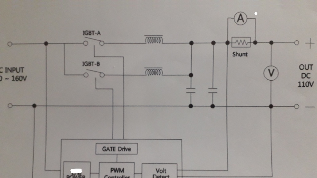

120337


It has following properties,

1. Input is 120 to 160 volt DC/ 30 Amp.
2. Output must be 110volt/30 amp(maximum). +- 5% regulation( contineous output should be 20 amps)
3. Isolated in both input and output circuit.

4. Shunt sensing.

5. proper feedback.

6. 2 switches gets OFF/ON alternately.

7. May be soft switching.

8. May be 90% efficient.


I am thinking to modify it because bulky reactor/coupled inductor.
It has high current application.

kindly suggest a design that has

1. Less switching losss.
2. Less stress on switch.
3. Less number of component.
4. ZVS or ZCS idea.
5. Suitable ripple minimization.
6. Suitable couple inductor design.
 
Why coupled inductor? Why not independent two inductors?
3. Isolated in both input and output circuit.
Isolated I understand but both input and output?
120 to 160 volt DC/ 30 Amp. Output must be 110volt
When the input is 120V and the output is 110V there is not much headroom. The duty cycle will approach 100%.
2 switches gets OFF/ON alternately.
You need to explain how this works. I do not see how this helps you.

Please show phase between the two inductors.
 
Last edited:
Take a look on this transformer that is been used in this design. I think, posted diagram is wrong and confusing. Right at this moment it looks like pull- push or half bridge or flyback type.


120359
 
Is this a school project?
There is almost no information on the transformer and I don't see how it fits into the "Dropper'.
 
Is this a school project?
There is almost no information on the transformer and I don't see how it fits into the "Dropper'.

I beg pardon, if its still looks nonsence!
But believe me, it makes money!

This means a transformer requires to be used.
Transformer switchmode topologies include push-pull, half bridge, and full bridge.

Either ZVS or a ZCS are suggested for the higher power bridge topologies, but they are technically challenging.


Forget this nonsence diagram and think a flyback type buck converter, cant you see primary side contains 80 turns while secondary has 37!
 
I see you posted the same question on at least 3 forms. I hope you find the answers you want.
Where did you get the picture from in post #1?
 
I see you posted the same question on at least 3 forms. I hope you find the answers you want.
Where did you get the picture from in post #1?

I was walking on track, suddenly I got a piece of paper that was washed out by rain!
May be it was kind of manual / datasheet !
 
I built a coupled buck supply just for fun. (using SPICE)
It does work without diodes.
The voltage stress on the MOSFETs is 2X what you might think. Normally with a Vin=160V max you would think 161V is all the MOSFET will see. But I see 320 volts in the main body of the signal if there was no ringing. I see current in the MOSFET internal diode.
Results. You need two MOSFETs of 2x to 3x the voltage but you have no diodes. Probably it would be better to have one MOSFET that only sees 160V and add the diode. For the inductor you need two wires not one so the resistance will increase. One inductor will have less dc loss and defiantly less ac losses.
I also see a 400V MOSFET is slower, with higher ac losses. PLUS With 2x higher voltage the switching losses are 2x higher. 1.4x2=2.8 higher ac losses.

It is fun to see how the current flows in the off MOSFET, but I don't see how " it makes money!".
 
OK it has MOSFET current and looks like it is working but it is not.
I think this circuit is a joke. It looks good but I can not get any power out of it. Current circulates in the inductor and nothing goes out.
If I un-couple the inductors and add the diodes it works.

At start up there is 0V but even when I force an output voltage it makes no difference.
Vin=100V, IGBT-A closed. IGBT-B open at -100V, current flows through the top inductor through the caps back to Vin.
When IGBT-A is opened the current stored in the inductor "flybacks". This forces current to flow backwards through IFBT-B and this current runs back into the Vin supply. It is funny to see the IGBT current is negative 1/2 the time. Vin current (average) is zero.
The current in the output capacitors rumps positive 50% of the time and negative 50% of the time. So the voltage at Vout does not move.
120414

Remember the inductor is coupled (or center-tapped).
If I start out with 50V on Vout: then the voltages are +100V----50V----0V. When the IGBTs change state it is 0----50---+100. The 50V is constant. I can reach in and manually increase or decrease the Vout voltage and it is easy to move.
------------------------------
If the phase is reversed in the inductor then the two IGBTs and the two inductors really are in parallel and need a diode(s) or they will overvoltage.
---------------------------------
either some one really understands power supplies and has played a joke
OR
some one dose not understand power supplies.
OR
Something big is missing.
 
Dear Sir Ronsimpson,
I do appreciate your analysis and effort you did here!

Yeap! This circuit is nonsense indeed.
Because of ...

1. No freewhiling path/ diodes.
2. Energy storing device alignment is wrong for sure.
3. Inductors are parallel, means it fails to describe wheather its bridge type or flyback type.
4. In this application, user must think a power transformer with center tap winding in sencondary!

5. CCM or DCM mode circuits cant be explain, because stupid circuit path.


Lets move our mind from this design to this follwing one ( its from a knowledgeable researcher)


120415


Can you feel anything clear from it?

1. Input coupled inductor maintains isolation?
2. For the ON/ OFF of switch( Mosfet/ igbt/)
, free whiling paths is notiable.

3 . More simple that might not require ZVS, ZCS.

4. Gain equitation can be possible to find.

5. Interesting to see how the parallel capacitor shows the advantage.

6. For this kind of high current application, not sure the switch would be long lasting or the inductor size!


What do you think sir?
 
More simple that might not require ZVS, ZCS.
Most buck supplies do not have Cr. It is there to slow down the switching edges. Probably the edge is 25nS with no cap and 100nS or 200nS with the cap. This solves some AC losses.
If no Lr; When the MOSFET turns on it must reverse D0 and lift up. During the switching time there is both voltage and current on the MOSFET, so there is power loss.
With Lr; Whe the MOSFET turns on there is no current in Lr so the switch closes with no load. Much less switching losses. After the MOSFET closes the current in Lr ramps up fast (small value for Lr). When the Lr current equals Lf current the center node is pulled up softly. Now there is no voltage across Lr1. When the MOSFET opens up the energy stored in Lr1 is returned back in Vs via Lr2.
120420

Soft switching, high frequency, low RF radiation, zero switching.
 
Nice explanation !

It is resonant. "Cr" is the clue. Cr is much much smaller than Cf. Also "Lr"
Well, if its resonant then are you considering the whole coupled inductor Lr at a time ?
In this whole circuit, can you see more LC? If the switch S is terned ON, Lr1 pole gets positive while Lr2's pole is negative, at this point what benifit from Lr1 and Cr we are getting? At this moment load can see the "input impedance ?


Most buck supplies do not have Cr. It is there to slow down the switching edges. Probably the edge is 25nS with no cap and 100nS or 200nS with the cap. This solves some AC losses.
Yeap, make sense. Cr is discharging/charging at this time?
AC losses are from inductor magnetic flux ( may be in coupled inductor mafnetic flux cancelled), otherwise across the switch! That may suppress by Cr you said.


If no Lr;
When the MOSFET turns on it must reverse D0 and lift up. During the switching time there is both voltage and current on the MOSFET, so there is power loss.
Reseaonable consideration indeed. This time can Lf wish to charge ?

; Whe the MOSFET turns on there is no current in Lr so the switch closes with no load. Much less switching losses. After the MOSFET closes the current in Lr ramps up fast (small value for Lr). When the Lr current equals Lf current the center node is pulled up softly. Now there is no voltage across Lr1. When the MOSFET opens up the energy stored in Lr1 is returned back in Vs via Lr2.

Really fantastic !
At this time D0 and D1 are conducting, freewhiling , while Lf may be discharging.
System completes safe mode!

Dont you think it can be usable for previous requiement in post 1# ?
It might have power loss, but not sure from previous one.

Since we introducing 2 inductor, cant we make lighter one?
Fast and high frequency and current application, MOSFET is must?

I will simulate this circuit, for the switching controle and monitoring need to think more.
 
One more comment:
The diagram is something a professor at school thinks up. It is very hard to drive a MOSFET when the Source switches from below ground to supply very fast. The Drain also switches from ground to supply. "In theory it works"

I moved things around and got the MOSFET on ground so it can be produced.
OR
Found a way to drive the gate. Crazy Gate drive that I have used.
----------------------------------------------
With soft switching; usually there is a limited range of power. Maybe it is good for 1 to 2A but does not soft switch below 1A. I have only used soft switching where I knew the power will never go to zero.
----------------------------------------------
The supply is not full resonant. Only the edges are resonant.
 
The diagram is something a professor at school thinks up. It is very hard to drive a MOSFET when the Source switches from below ground to supply very fast. The Drain also switches from ground to supply. "In theory it works"

Yes, sure. Second design is also a very basic one ! But proffesor wanted to save the switch. Dont you think there is some advantage using "High side" ruther then "Low side"?

With soft switching; usually there is a limited range of power. Maybe it is good for 1 to 2A but does not soft switch below 1A. I have only used soft switching where I knew the power will never go to zero.
Not sure what you have want me to tell. Are you talking about the Switch itslef/its operating current range or the input power of the buck converter ?

Found a way to drive the gate. Crazy Gate drive that I have used.
The initial stupid design is also run by gate driver.

The supply is not full resonant. Only the edges are resonant.
Could you tell me why people care about resonance in converter ? For the maximum power transfer.


Anyway, let me know what dificuilties may arise to use the second design in case of previous power requirment!
Talk about more for isolation in buck converter, why people get more advantage using Bridge type, Flyback, SEPIC and so on ,,,,

Even the boost operation, kindly take a look the research paper in this attachment
 

Attachments

  • kosai2009 .pdf
    273.6 KB · Views: 193
why people care about resonance in converter
For many years we built power supplies with 1000 volt or 1500 volt transistors. They are slow parts because HV silicon is slow. Most of my life there was no HV Schottky diodes.

For now think Buck supply, where there is a transistor and diode across the input supply.
Normal diodes have a Reverse Recovery Time. It takes time for the diode to open up. If you are running 10A in the diode, just removing the current will not allow the diode to have voltage across it. A large HV diode might take 10A for 1uS for the diode to have voltage across it.
Time 1) "off time" Diode is conducting. 10A 1V =10 watts. Power loss in the diode. (HV diodes have a high forward voltage)
Time2) "Turn on" the transistor. The transistor must lift the 10A output current PLUS for the RR time it must pull open the diode. 10A load + 10A diode current X 1000V = 20,000 watts for 1uS.
Time 3) "on time" Now the diode is open and no diode current. Transistor = 1V x 10A = 10 watts.

So we made these supplies "resonant" and not buck. There is a capacitor across the diode. The capacitor is sized to slow down the voltage as it goes from 0 to supply. I usually wanted the voltage to increase to 10 or 20V during the transistor's turn on time/turn off time. Transistor's current goes from 0 to 10A (or 10 to 0) while the capacitor controls the voltage from 0 to 10V. The power loss in the edge is 1/100. Because the ac losses are much less we can run faster.

I worked with a man that was doing this before WW2. (before transistors) When I started we did this at 15750 and 17,000hz. When I stopped that business we ran at 125khz. Now these high voltage parts are all gone. Using low voltage silicon we do 2mhz power supplies.

"Cross over time" is the time when you have both voltage and current on the silicon. For this time the power loss is very high. Any type of resonant switching helps this but makes the supply more complicated, harder to design, adds more Ls and Cs, and restricts the input voltage range and output current range.

Graph of transistor from data sheet. There is a time where voltage is high and current is high. Cross Over Time This happens for turn on and turn off. This graph is for turn off. This is where the silicon-ac losses happen.
120432
 
Last edited:
They are slow parts because HV silicon is slow
There should be "solid state physics" why silicon is slow in manner. During HV what would be the configuration of semiconductor ? In high temperature, meaning that high voltage or current why they should sustain? What matters for PNP or NPN junctions?

Normal diodes have a Reverse Recovery Time. It takes time for the diode to open up
Can you post a equation, that has exponential factors and time delay ?

It takes time for the diode to open up. If you are running 10A in the diode, just removing the current will not allow the diode to have voltage across it. A large HV diode might take 10A for 1uS for the diode to have voltage across it.
Time 1) "off time" Diode is conducting. 10A 1V =10 watts. Power loss in the diode. (HV diodes have a high forward voltage)
Time2) "Turn on" the transistor. The transistor must lift the 10A output current PLUS for the RR time it must pull open the diode. 10A load + 10A diode current X 1000V = 20,000 watts for 1uS. Time 3) "on time" Now the diode is open and no diode current. Transistor = 1V x 10A = 10 watts

Speachless!! what a explanation!
could you post a simple circuit for this application? Can we imagine last S and D0?
If the volatge/current (not zenar may be) raise for long time in diode, what could happen!!
Beside powerloss things might require "stability". I feel a close connection for OFF time and ON time of diode and transistor while thinking for a inductive load!
Both has PN or NP in common, but transistor has control for the conduction wheather its use as a switch!

The capacitor is sized to slow down the voltage as it goes from 0 to supply
Yeap, so I have made an conversation on that converter.
People can calculate switching loss for a IGBT, MOSFET, Transistor, FET etc.
why dont we think about using less number of component!
let me study your figure !
 
Status
Not open for further replies.

Latest threads

New Articles From Microcontroller Tips

Back
Top