Good afternoon,
First post here and bring an exciting analog design challenge of power electronics mixed with RF") .
.
As you know measuring with an oscilloscope the ON-state voltage of a transistor is very challenging as the dynamic range (tens of mV to hundreds of volts) is very large and regular passive probes along with oscilloscopes don't have sufficient capabilities/bits to address this task. They cannot measure high voltages and very low voltages at the same time. People have built tons of ON-state voltage measurement circuits (OVMCs) for clipping the OFF-state voltage mainly through Schottky or Zener diodes so that a custome probe only measures the ON-state voltage. Here an example of the results of a commercial product:

However, all circuits, like this one, face the same issue... They are blind in the switching time due to their limited bandwidth. This is due to the recovery time of this clipping diode which can be large and, if an amplification circuit is needed, also the desaturation of the opamp. The bandwidth of the the OVMCs is normally aprox. 50MHz while the switching harmonics can get to 500MHz in new generation power devices (GaN and SiC).
I have been thinking on a different strategy by using a high frequency logarithmic opamp where no clipping or saturation is made at all and the entire dynamic range is measured in one custome probe. OFF-state high voltage would be highly attenuated while ON voltage would be amplified. There would be no clipping or saturation of the opamp. However I am not sure about the feasability of this design.
My target device under test (DUT), for how challenging it is, would be the EPC2088 GaN (100V@3mOhm) device going up to 80V with currents from 1A up to 20A and measuring it with the 50 Ohms input of the oscilloscope (12 bits, max 5V). This kind of transistors can have rise/fall time of 2ns. I have already built and validated a prototype of half-bridge (for measuring it in real operation) and a PCB for testing the classical methods and even a basic discrete log amp amplifier but would like to know your opinion.
I am mainly worried about the worst case of 1A for this 3mOhm device. This would equal to 3mV and our probe should measure up to 80V. I have thought of placing some large power resistor in paralel with the DUT to attenuate all voltages and face this with a regular high performance opamp but low voltage level would be very close to the noise levels.
I have also seen some information from Analog Devices of High Frequency Log Amps with integrated circuits like the AD8306S but not sure with the could stand that high rise/fall times in the inputs.
Any recommendations?
Found this task feasable?
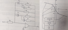
My generic design comes with the LTC6269-10 opamp, BFP460 NPN bipolar transistors and BAT54K for the Schottkies (this circuit would be able to perform multiple OVMC, the temperature effect on the NPN is not compensated in this circuit as it is made for concept validation):

I also attach one example of working LTspice simulation with the DUT and an example of clipping OVMC with a Schottky diode and a amplification circuit for the 50 Ohms oscillocope reading.
Would very great if you could provide you your insights about this challenge.
Best regards,
José Miguel.
First post here and bring an exciting analog design challenge of power electronics mixed with RF
.As you know measuring with an oscilloscope the ON-state voltage of a transistor is very challenging as the dynamic range (tens of mV to hundreds of volts) is very large and regular passive probes along with oscilloscopes don't have sufficient capabilities/bits to address this task. They cannot measure high voltages and very low voltages at the same time. People have built tons of ON-state voltage measurement circuits (OVMCs) for clipping the OFF-state voltage mainly through Schottky or Zener diodes so that a custome probe only measures the ON-state voltage. Here an example of the results of a commercial product:
However, all circuits, like this one, face the same issue... They are blind in the switching time due to their limited bandwidth. This is due to the recovery time of this clipping diode which can be large and, if an amplification circuit is needed, also the desaturation of the opamp. The bandwidth of the the OVMCs is normally aprox. 50MHz while the switching harmonics can get to 500MHz in new generation power devices (GaN and SiC).
I have been thinking on a different strategy by using a high frequency logarithmic opamp where no clipping or saturation is made at all and the entire dynamic range is measured in one custome probe. OFF-state high voltage would be highly attenuated while ON voltage would be amplified. There would be no clipping or saturation of the opamp. However I am not sure about the feasability of this design.
My target device under test (DUT), for how challenging it is, would be the EPC2088 GaN (100V@3mOhm) device going up to 80V with currents from 1A up to 20A and measuring it with the 50 Ohms input of the oscilloscope (12 bits, max 5V). This kind of transistors can have rise/fall time of 2ns. I have already built and validated a prototype of half-bridge (for measuring it in real operation) and a PCB for testing the classical methods and even a basic discrete log amp amplifier but would like to know your opinion.
I am mainly worried about the worst case of 1A for this 3mOhm device. This would equal to 3mV and our probe should measure up to 80V. I have thought of placing some large power resistor in paralel with the DUT to attenuate all voltages and face this with a regular high performance opamp but low voltage level would be very close to the noise levels.
I have also seen some information from Analog Devices of High Frequency Log Amps with integrated circuits like the AD8306S but not sure with the could stand that high rise/fall times in the inputs.
Any recommendations?
Found this task feasable?
My generic design comes with the LTC6269-10 opamp, BFP460 NPN bipolar transistors and BAT54K for the Schottkies (this circuit would be able to perform multiple OVMC, the temperature effect on the NPN is not compensated in this circuit as it is made for concept validation):
I also attach one example of working LTspice simulation with the DUT and an example of clipping OVMC with a Schottky diode and a amplification circuit for the 50 Ohms oscillocope reading.
Would very great if you could provide you your insights about this challenge
.Best regards,
José Miguel.