Hi Merv,
<applause> @ Merv")
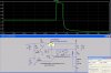
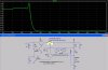
Yes, very good Merv, that looks like a good solution, one which i think i can use.
A slight improvement is possibly to add a second transistor, NPN, base driven by the first one's collector, emitter to ground, collector to the output of the LM317. Not too much more complexity to pull the output to zero on a fault (or whatever the LM317 really defaults to with a near short on the output). The first transistor forces current through the second, the second shunts the output directly to ground. That should take care of the +2.1v problem (although that isnt really too bad either).
I havent tested this yet though If you already have a sim set up, perhaps you would care to try it.
The only problem left now (not truely a problem, just an inconvenience) is that this (and other) solution(s) require a 2k pot to get quite good adjustment ranging (actually very good, spread nice and evenly over the full voltage range) and although that isnt impossible, it would be nice to be able to use a 10k pot with this.
Not truely a necessity i guess though.
Thanks for the idea! I have a feeling that this idea increased your so called "reputation" he he.
BTW, some capacitance on the ADJ terminal to ground is usually a good idea anyway, as much as 10uf even, that helps reduce ripple. I would be using some capacitance on that terminal anyway because of that and to keep any static from the pot arm from bothering anything.
<applause> @ Merv
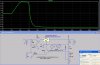
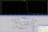
Yes, very good Merv, that looks like a good solution, one which i think i can use.
A slight improvement is possibly to add a second transistor, NPN, base driven by the first one's collector, emitter to ground, collector to the output of the LM317. Not too much more complexity to pull the output to zero on a fault (or whatever the LM317 really defaults to with a near short on the output). The first transistor forces current through the second, the second shunts the output directly to ground. That should take care of the +2.1v problem (although that isnt really too bad either).
I havent tested this yet though
If you already have a sim set up, perhaps you would care to try it.The only problem left now (not truely a problem, just an inconvenience) is that this (and other) solution(s) require a 2k pot to get quite good adjustment ranging (actually very good, spread nice and evenly over the full voltage range) and although that isnt impossible, it would be nice to be able to use a 10k pot with this.
Not truely a necessity i guess though.
Thanks for the idea! I have a feeling that this idea increased your so called "reputation" he he.
BTW, some capacitance on the ADJ terminal to ground is usually a good idea anyway, as much as 10uf even, that helps reduce ripple. I would be using some capacitance on that terminal anyway because of that and to keep any static from the pot arm from bothering anything.
Last edited: