Continue to Site

Welcome to our site!

Electro Tech is an online community (with over 170,000 members) who enjoy talking about and building electronic circuits, projects and gadgets. To participate you need to register. Registration is free. Click here to register now.

  • Welcome to our site! Electro Tech is an online community (with over 170,000 members) who enjoy talking about and building electronic circuits, projects and gadgets. To participate you need to register. Registration is free. Click here to register now.

Kaneda Amp

Status
Not open for further replies.
Dear forum members,
A Kaneda amplifier was built a while ago, but is oscillation sensitive.
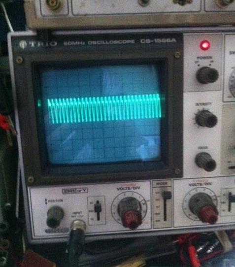
Tried to place a capacitor in parallel via the negative feedback resistor 10 k, but that actually caused oscillation 0,5 uS.
How can I contain this amplifier in the high frequencies, it now runs up to 380 Khz, but it also sounds quite fierce in the high ranks.
Sincerely,
Pim
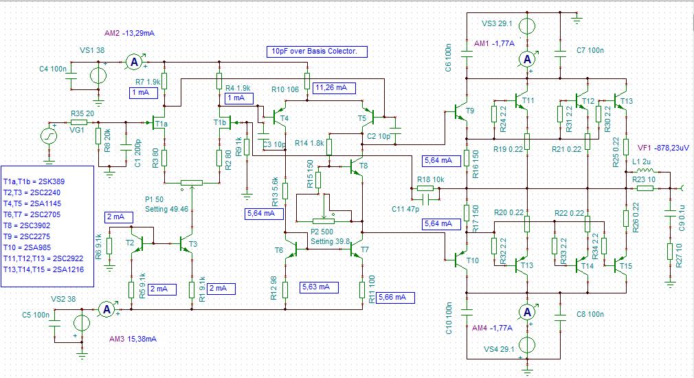
ScreenShot492.jpg
ScreenShot490.jpg
 
You have provided zero information about the amplifier's intended operating characteristics, but my guess from the three output transistors in parallel is that you are moving a large amount of current. Many (most?) amplifier oscillation problems are caused by inadequate power supply decoupling and/or incorrect or insufficient grounding. If the input stage ground current shares a wire or trace with the output current, that is a positive feedback path. Same for the +/- power supply runs.

Also, if the board is single-sided and has no ground plane, that is another common cause of problems.

ak
 
my first question is... does the oscillation make the amp draw more current? if so, then increase the value of C2 and C3, which are your compensation caps. if the oscillation doesn't make the amp draw more current, then check the idle current of the output transistors. if it's near zero, then the oscillation is being caused by the feedback trying to compensate alternately for a +0.7V and -0.7V offset. there's a "dead zone" with the idle current at zero, and that can lead to oscillation, and increasing the integrating capacitance across the feedback resistor will only make the oscillation worse.

according to your simulation, the idle current is 1.77A, which is much too high at about 500mA per device. 15-50mA is about where the idle current per device should be.
 
Last edited:
Also, if the board is single-sided and has no ground plane, that is another common cause of problems.
there are plenty of amps built without a ground plane on the PCB that work just fine. the layout for this board looks ok, as long as the speaker grounds originate in a star ground at the power supply and aren't tapped off the board. the board even has the feedback taken from the center of the output track.
 
How did you make L1/R23? Insulated wire over a carbon composition resistor?

Put a 0.1 uf 50 V metalized film cap between C and E of T8.

What do the currents look like without a signal?

C6, C7, C8 and C10 Two of these should be about 100 uF at 100 V electrolytic caps, not 100 nF.
 
Last edited:
How did you make L1/R23? Insulated wire over a carbon composition resistor?

Put a 0.1 uf 50 V metalized film cap between C and E of T8.

What do the currents look like without a signal?

C6, C7, C8 and C10 Two of these should be about 100 uF at 100 V electrolytic caps, not 100 nF.
It is an air coil that is parallel to a metal film resistor.
ScreenShot504.jpg
 
Dear Forum Members
On this schedule I have signed the changes made by forum members, if there are any sugestions please bring them up.
Kind regards,
Pim
ScreenShot506.jpg
 
Here the ground diagram of the amplifier.
As an attachment.
 

Attachments

  • Aardplan Kaneda Versterker 23 juli 2019.pdf
    744.8 KB · Views: 363
your Zobel network (C9, R27) should be connected on the "inboard" side of the inductor, not the outside. with it connected on the outside you have a low Q series resonant circuit driven by the amplifier, which is resonant at 356khz (which is very close to the 380khz you wrote in the first post). since the feedback is tapped from the inboard side of the coil, it's isolated from the Zobel network by the coil.

might i recommend also, that while troubleshooting your oscillation problem, use a current limited power supply instead of the brute force supply. that way you can troubleshoot the amplifier without worrying about smoking anything. with the idle current set properly, a limit of 100-200mA should be enough to run the amp board with no load, and not risk any pyrotechnics.

for an in-depth tutorial on amplifier instability [this LTC app note] talks about several different causes of instability, and how to cure them. the biggest and best takeaway i got from this app note was that the biggest cause of instability in amplifiers is the speed mismatch between the input stage and output stage. but all of the causes of instability are described in this app note.
 
why is that op amp (upc1234) not in the schematic? or is that 1237? that would make it a protection ic.... which begs the question,,, where's the rest of the amp?
 
Last edited:
or are you telling us the RC network and RL network aren't on the amplifier board? they should be...
 
also, after looking at the diagram for your ground connections, it looks like you have star connections between the capacitors, which is good, but some of the other ground connections are branched, and the amp ground goes back through another board with a ground. if there's current between the two ground points on the power supply, and the amplifier ground is on the far side of that voltage drop (when you have current flowing through a wire or PCB trace, the very small resistance develops a voltage across it, and one end is no longer truly at ground potential), the ground reference for your input stage has changed, and that can cause oscillation. the amplifier ground should go directly to the "star" ground between the power supply caps. there should also be two separate speaker grounds going back to the star ground. there are books about amplifier design that cover the whole subject of ground systems, what works, and what doesn't work.

ground layouts can be tricky to get right, and probably has a lot to do with the opinion that many engineers have that "audio design is a black art". even in the 21st century, receivers and amplifiers go into production, and within a month of the equipment hitting the market, manufacturers come out with a flurry of ECO's (engineering change orders) and modifications of "cut this PCB trace and run a heavy gauge piece of wire from point "A" to point "B". "
 
The security is not there because there is no part in the library of tina software.
There is also no image of the power supply stage on the diagram, here the power supply and the protection, power supply + and -.
The minus side is the same.
ScreenShot518.jpg

ScreenShot515.jpg

ScreenShot516.jpg

Ground has changed.
ScreenShot508B.jpg
 
Status
Not open for further replies.

Latest threads

New Articles From Microcontroller Tips

Back
Top