Continue to Site

Welcome to our site!

Electro Tech is an online community (with over 170,000 members) who enjoy talking about and building electronic circuits, projects and gadgets. To participate you need to register. Registration is free. Click here to register now.

  • Welcome to our site! Electro Tech is an online community (with over 170,000 members) who enjoy talking about and building electronic circuits, projects and gadgets. To participate you need to register. Registration is free. Click here to register now.

Instrumentation Amplifier and PIC ADC

Status
Not open for further replies.
OK, maybe I'll just ditch that idea and go with VREF = VCC/2. Did you see my edit to post #37?

Also, I was mistaken about having a bunch of MCP6002s. I have MCP619s. I think they should work just as well for my purposes though. Thoughts?

hi,
The MC619 has better input offset and noise figure than the MCP6002, so it should perform well in the circuit.

IIUC you have some 1K 1% resistors, I would use those instead of the NTE952. The Vref using may not be precisely 2.500V, see image.
The 1K divider Vref should track the Vext to the bridge, the MCP3204 is a ratio metric adc.
The NTE adjust pin, is used to add resistors in order to improve the temperature tracking.

NOTE: on some 2.5Vref devices ie: TL431 for example, the Vref can be changed by adding resistors from +Vs and 0V to the adjust pin.

The d/s for the NTE952 is not clear regarding the Vref change on using adjust.
 

Attachments

  • AAesp01.gif
    AAesp01.gif
    10.3 KB · Views: 181
Last edited:
The d/s for the NTE952 is not clear regarding the Vref change on using adjust.

Hey Eric,

NTE data sheets are the worst. It's so annoying when I go to a store and that's all they carry. At any rate, I took your suggestion and used 2 1kΩ/1% resistors to set a 2.5V reference voltage so no NTE952 for me.

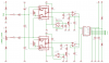
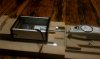
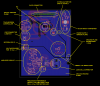
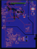
I apologize in advance for this gargantuan post but I was pretty busy yesterday and there's lots to discuss. First off, I expanded the test circuit and it is much improved. I attached the latest schematic.

The differential signal coming from the load cell can be either positive or negative depending on whether the load cell is experiencing compression or tension. Since this is a single supply circuit I have two INA118Ps in parallel. One is inverting and the other non-inverting and each one goes into its own ADC channel. The PIC retrieves both channels one at a time and after some math, figures out the applied load and the direction (i.e. push or pull). It works pretty well right now. I have the PIC talking to the MCP3204 and displaying the values on an LCD.

After hooking everything up, I adjusted the offset voltage pots (R5 and R10) so that each ADC channel output 100 counts with no applied load. I then loaded the load cell in compression with 50 pounds and adjusted the gain pot R2 until the first channel of the ADC output 4050 counts. I repeated that step in the tension direction for the second channel while adjusting the gain pot R9.

The PIC then does some math. Here is a simplified form:

force = 50*(ADC_CH0 - ADC_CH1)/(4050-100)

The PIC determines direction by looking at the sign of force.

So as I stated, it works fairly well but there are still 2 aspects of the circuit with room for improvement.

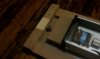
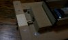
The first is signal noise. I already have the PIC doing a running average calculation of the last 5 measurements but still, without touching anything and just watching the ADC value it jumps around a lot. Sometimes as much as 20 or 30 counts in either direction. It's hard for me to tell right now the source of the noise. I'm sure my home made power supply isn't that clean. Also, the entire circuit right now is in a solderless bread board with wires going everywhere. On top of that, it's plugged into my development board so, there's probably a lot of digital switching noise in there too.

I'm sure if I follow good practices, the performance will improve after I design the board and build the circuit. I found this pretty handy application note, AN688 - Layout Tips for 12-Bit A/D Converter Application. Also, once in the final circuit, the analog portion will be powered with a precision 5V reference. Right now it's just a 7805 powered by my bench power supply. So I know the signals will be more stable but just how much more, I have no idea.

Because I won't know until after the board is put together, I'm thinking about designing in some low pass filters. Ideally, I would have 1 filter at the input of the INA118P, 1 at the output, and 1 at the reference voltage input. That would be 3 per amplifier for a total of 6 low pass filters.

Since the offset voltage and INA118P output are already being buffered with op amps, I was thinking I could just add some resistors and capacitors and make them into unity gain low pass filters. For the input of the INA118P, I was thinking about using a dedicated low pass filter IC. After looking around a little, the MAX7426, the TLC04, or the TLC1062 seem to fit the bill pretty well.

Do you have any thoughts on this approach? Do you think this is overkill?

The second area for improvement is non-linearity. At 0 and at 50 lbs, the output matches the applied load. But in between, it can be off by as much as 1.5 lbs. I'm unsure of the source of this non-linearity. The load cell data sheet states that the non-linearity is ± .02% of full scale. So that would be ± .01 lbs, not 1.5lbs. I did get the load cell on the cheap so it wouldn't surprise me is it was out of spec but that is way out of spec. I know also that the INA118P and the MCP619 output buffer can introduce some non-linearity but I'm unsure how significant their contribution is. I know that I can compensate for this in software via a transfer function, but I'd like to minimize all sources of error due to non-linearity before doing that.

Do you have any thoughts in this area? How can I minimize this error?

I think that's about it for now. Thanks again for your thoughts and ideas. They are most helpful.
 

Attachments

  • INA118P Test Circuit 3.PNG
    INA118P Test Circuit 3.PNG
    67 KB · Views: 546
hi vne,
Have download your circuit and app note, will look thru your test circuit.

The problem with such low level signals is 'noise', good layout is essential, also is the isolation of the analog from the digital circuitry on the pcb.

Are you planning to use the L/C over a +/-50 lbs range.? ,
if so, is the non linearity over 50 lbs range the same for tension and compression loads.?
also what are you using to apply the load to the cell, calibrated weights ???

I guess you will be averaging a number of samples from the ADC , in the PIC program in order to create an average figure.?
also what is the planned sampling rate of the ADC readings.?

I would recommend that you convert the OPA buffer to an low pass active filter.

Sorry I have so many questions.
 
Sorry I have so many questions.

Not at all. It is you who is doing me a favor. I don't mind the questions.

The problem with such low level signals is 'noise', good layout is essential, also is the isolation of the analog from the digital circuitry on the pcb.

I have been doing a lot of reading on the subject of separating analog and digital grounds but unfortunately, I haven't been able to find a reference that gives any sort of concrete rules on the matter. From my reading, the consensus seems to be that separation of the analog and digital ground planes can introduce some problems so it should only be done if need be. The problem is, I don't know if I will need to do it or not until after the PCB is made and I'd like to only do that once. Also, I'm uncertain on exactly how to tie the two grounds together. A small value capacitor? Resistor? Ferrite bead? Once again, I haven't found any firm guidance on this.

Before you asked me this question, I was planing on using a single ground plane for both digital and analog portions. I had planned on using a double sided PCB with one side having surface mounted components and traces. The other side I would make ground and keep it mostly solid copper with as few breaks in it as I can manage. To minimize noise from the digital portion I had planned to physically separate the analog and digital circuits and make all the analog traces as short as possible. Basically, I was going to lay everything out consistent with that application note I linked to in my previous post.

What do you think about that plan?

Also, the application note talks about using a digital buffer. Do you think I should use a digital buffer for my SPI lines in between the PIC and MCP3204? If so, can you suggest an appropriate IC?


Are you planning to use the L/C over a +/-50 lbs range?

The requirement I was given was for a ± 50 lb range but it practice, it will only see about ± 35-40 lbs.

is the non linearity over 50 lbs range the same for tension and compression loads?

Yes, it's pretty close.

also what are you using to apply the load to the cell, calibrated weights???

I made a test and calibration stand out of mostly MDF and plywood. It loads my load cell against a commercially purchased hand held spring scale that I signed out from work. The spring scale is what's currently being used in the factory and the plan is to have my device replace it. I realize that by using this approach, my device will only be as accurate as the spring scale but it is professionally made, expensive ($650 USD), and within its calibration period. So, I think it will be good enough. Also, I'm going to prove to the powers that be that my device is accurate by checking it against the currently used spring scale. I think I'll have a tougher sell if my device doesn't match the spring scale and then I try to convince them my home brewed thingamajiggy is correct and their scale is not.

I'll post some pictures of my test set up after I get home tonight so you'll have a better idea of exactly what's going on.

I guess you will be averaging a number of samples from the ADC , in the PIC program in order to create an average figure?

Yes, right now it's 5 samples but I can do more or less if need be.

What is the planned sampling rate of the ADC readings.?

I don't know exactly. I'm writing the code in C and I haven't gone through each line to add up the clock cycles. I put in a 5 ms delay between the reading of the first ADC channel and the second so if I had to guess, I'd say that currently it's sampling at 100 - 200 Hz. I wouldn't want to go much below 25Hz though.

I think there is some built in debugging tool with the IDE I'm using that can tell the user how much time is in between different points of the code. I'll see if I can figure out how to work it.

I would recommend that you convert the OPA buffer to an low pass active filter.

I'll do that when I get home tonight and see how things improve. Unless you have any objections, I was thinking I would use a Sallen-Key Butterworth low pass filter like the one on page 16 of the application note SLOA058 - A Single-Supply Op-Amp Circuit Collection. I was thinking about a 10 Hz cut-off frequency, or lower if I can get it. By the way, do you have any idea what the variable 'p' is in the equation to the left of the circuit?
 

Attachments

  • IEEEGrounding.pdf
    128.5 KB · Views: 167
  • layout.pdf
    153.3 KB · Views: 132
  • doc0999B.pdf
    95.5 KB · Views: 344
Last edited:
So here are some pics of the test stand. It's basically just a big piece of MDF that forms the base. On one side of the base I bolted the commercial spring scale I'm using as a reference. It is fixed in place. I bolted my project to a smaller piece of plywood and placed it on the other side. The plywood is not bolted to the base but instead slides back and forth inside 2 pieces of aluminum C-channel that act as tracks. The scales' rods have threaded ends and are connected by a coupling nut when testing. Finally, the whole mess is compressed or stretched by turning the drive screw at the far end with a wrench. You can see it in some of the pictures. The drive screw threads through a floating nut plate that's inside the big block of wood mounted directly behind my project.
 

Attachments

  • 1.jpg
    1.jpg
    1.1 MB · Views: 220
  • 2.jpg
    2.jpg
    1.2 MB · Views: 187
  • 3.jpg
    3.jpg
    1.4 MB · Views: 177
  • 6.jpg
    6.jpg
    1.2 MB · Views: 202
  • 5.jpg
    5.jpg
    1,013.7 KB · Views: 168
  • 4.jpg
    4.jpg
    924.5 KB · Views: 158
  • 7.jpg
    7.jpg
    1.3 MB · Views: 189
  • 8.jpg
    8.jpg
    912.1 KB · Views: 189
I made some modifications to the test circuit last night (schematic attached). The first thing I did was download the TI filter design tool you recommended. It is really cool. Much better than the Microchip equivalent. I had it generate a Sallen-Key Butterworth low pass filter. I used a pass band of 10 Hz and a stop band of 400 Hz. That was the lowest stop band I could input and still have it generate a 1 stage filter design. Instead of replacing the 2 unity gain op amps I had as buffers between the INA118Ps and the MCP3204 (shown as IC3B and IC3D), I just added the filters in between them and the MCP3204. It was just easier to add to the circuit than it was to rip the other stuff out and replace them. The buffers aren't really doing anything and aside from introducing a little offset error, I'm pretty sure they're not hurting anything either. In the final circuit I plan to remove them unless you think that would cause any problems.

Upon powering up the circuit with the filters in place, I saw an immediate reduction in signal noise. Before the filters, the ADC values were jumping around sometimes by as much as ± 30-40 counts. After the filters, it was down to ± 10 counts.

The next thing I did was build up the power supply portion of the circuit so that I could take everything off of my bench power supply. I put together the DC-DC switching converter shown in the schematic and tuned it for an 8.5V output. That 8.5V feeds the 7805 to power the rest of the circuit. As expected, the switching action introduced some noise. At this point I was back up to a signal noise of ± 15-20 counts or so.

Next, I separated the ground for the batteries and DC-DC converter from the ground for the rest of the circuit with a .22Ω resistor. This improved things. I was back down to a signal noise of ± 5 - 10 counts.

Lastly, just to satisfy my curiosity, I unpowered the DC-DC converter and simply powered the entire circuit off of 6 AA batteries. This yielded the best results by far. With the filters in place and running off batteries only, the signal noise went down to an intermittent ± 1 - 3 counts.

So, it appears that things are coming together. I'm sure that if I follow good practices when laying out the PCB, I should be able to reduce the noise further. Hopefully to a level less than the LSB.

There are a few more tweaks on my list before arriving at the final circuit:

  1. Remove the redundant unity gain buffers in between the INA118Ps' outputs and the low pass filters.
  2. Add low pass filters before the inputs on the INA118Ps. I figure it can't hurt. Can it?
  3. Design the PCB to use the DC-DC converter but leave provisions to down grade to battery power only in the event I can't isolate the noise from the converter to an acceptable level.
  4. Increase the reference voltage of the MCP3204 to 3V and adjust the gain of the INA118Ps accordingly. With a properly filtered input to the INA118P, I hope the increased reference voltage and IA gain will help with the noise problem.
Do you have thoughts about any items in my list?

Aside from those few things, I think the circuit is just about ready. I'll make sure to study up and all the layout guideline information you gave me and then I'll start on the PCB.
 

Attachments

  • INA118P Test Circuit 4.PNG
    INA118P Test Circuit 4.PNG
    116.2 KB · Views: 357
There are a few more tweaks on my list before arriving at the final circuit:

  1. Remove the redundant unity gain buffers in between the INA118Ps' outputs and the low pass filters.
  2. Add low pass filters before the inputs on the INA118Ps. I figure it can't hurt. Can it?
  3. Design the PCB to use the DC-DC converter but leave provisions to down grade to battery power only in the event I can't isolate the noise from the converter to an acceptable level.
  4. Increase the reference voltage of the MCP3204 to 3V and adjust the gain of the INA118Ps accordingly. With a properly filtered input to the INA118P, I hope the increased reference voltage and IA gain will help with the noise problem.
Do you have thoughts about any items in my list?

hi,
Looks OK to me.:D

Personally I wouldn't add any more filtering to the IA inputs, the original drawing seemed to cover the recommended filtering.
 
hi,
Looks OK to me.:D

Personally I wouldn't add any more filtering to the IA inputs, the original drawing seemed to cover the recommended filtering.

OK, understand. I suppose I'll just rely on a properly laid out PCB to eliminate the last 1-3 bit counts worth of noise. Now it's time to make it happen. It will probably be few weeks before I have a mostly done PCB layout. I'll post it here when it's ready for some constructive criticism.

Thanks again for your contributions.
 
I've been pretty busy laying out the circuit board for this project and I think I'm almost done. I separated the board into 3 ground planes (analog, digital, and power supply). The digital and analog ground planes are each connected to the power supply ground plane through their own .1Ω resistors. I'm still a little fuzzy on the best approach for connecting the ground planes. I laid out all the analog and digital components physically separated on the board and I tried to route all the digital lines as far away from the analog portion as possible. The one thing I'm not really happy about is the placement of the Xbee transceiver. I would have preferred to have it a little further away from the analog amplifier circuit but I was kind of restricted in the layout by the enclosure size.

Anyway, here are some pictures of the board. I welcome your feedback as I'd like the analog portion to be as noise free as possible.

Thanks!
 

Attachments

  • Board_V1_Labeled.png
    Board_V1_Labeled.png
    221.9 KB · Views: 170
  • Board_V1_Top_and_Bottom_Populated.png
    Board_V1_Top_and_Bottom_Populated.png
    123.6 KB · Views: 163
  • Board_V1_Top_and_Bottom_Bare.png
    Board_V1_Top_and_Bottom_Bare.png
    100.5 KB · Views: 156
  • Board_V1_Top_Populated.png
    Board_V1_Top_Populated.png
    106 KB · Views: 152
  • Board_V1_Top_Bare.png
    Board_V1_Top_Bare.png
    84.7 KB · Views: 155
  • Board_V1_Bottom_Populated.png
    Board_V1_Bottom_Populated.png
    46.6 KB · Views: 155
I was looking through this thread and I wanted to comment on this post: https://www.electro-tech-online.com/threads/instrumentation-amplifier-and-pic-adc.118174/#post992065 I ran into a similar problem once. You need a resistor in series with pin 2 and pin 3 somewhere between 1 and 10K, I would guess, What happens is that Ib is dropped across a very small resistance and it causes an appreciable voltage drop. Any resistor will help. he higher the value, the higher the noise voltage.

You should have looked at the voltage between 1 and 2 and 3 and 8. Not sure if you would need a bias return path on pins 1 & 8 to ground. That would be a fairly large resistor to ground, so that Ib has a place to go.
 
I was looking through this thread and I wanted to comment on this post: https://www.electro-tech-online.com/threads/instrumentation-amplifier-and-pic-adc.118174/#post992065 I ran into a similar problem once. You need a resistor in series with pin 2 and pin 3 somewhere between 1 and 10K, I would guess, What happens is that Ib is dropped across a very small resistance and it causes an appreciable voltage drop. Any resistor will help. he higher the value, the higher the noise voltage.

The schematic in that post was wrong for a lot of reasons. One of the main mistakes I made was connecting both inputs to ground. I later ran across this statement from the datasheet.

"With single supply operation, VIN+ and VIN- must both be 0.98V above ground for linear operation. You cannot, for instance, connect the inverting input to ground and measure a voltage connected to the non-inverting input."

After reading that I changed the test circuit closer to this:

**broken link removed**

I then adjusted the pin 5 voltage with a buffered signal (not shown) until I got my desired null offset. That seemed to work pretty well.

You should have looked at the voltage between 1 and 2 and 3 and 8.

What should I have checked for here? The differential signal I'm amplifying is between pins 2 & 3. Pins 1 & 8 as far as I can tell from the data sheet are only for setting the gain.

Not sure if you would need a bias return path on pins 1 & 8 to ground. That would be a fairly large resistor to ground, so that Ib has a place to go.

Unless I missed it, the data sheet doesn't discuss that so I'm thinking that the bias current return path is taken care of internal to the IC and goes through the ground pin.
 
Usually, the difference between the inverting and non-inverting inputs is zero for an amplifier. It's the quick and dirty check. The 0.98 V above GND is pretty obvious as a reason it won't work.
 
Status
Not open for further replies.

New Articles From Microcontroller Tips

Back
Top