Continue to Site

Welcome to our site!

Electro Tech is an online community (with over 170,000 members) who enjoy talking about and building electronic circuits, projects and gadgets. To participate you need to register. Registration is free. Click here to register now.

  • Welcome to our site! Electro Tech is an online community (with over 170,000 members) who enjoy talking about and building electronic circuits, projects and gadgets. To participate you need to register. Registration is free. Click here to register now.

Instrumentation Amplifier and PIC ADC

Status
Not open for further replies.

vne147

Member
Hello everyone. Thanks in advance for your help. I’m seeking some advice for a project I’m working on.

What I’m trying to do is build a force measuring device. The force will be sensed by a 0 – 50 lb load cell (data sheet at bottom of post). The outputs from the load cell will feed the inputs of an instrumentation amplifier circuit. I’ll be building that circuit and it will be similar to the one in this thread:

Instrumentation Amplifier Circuit Question

The output from the IA will in turn feed into a PIC’s onboard 10-bit ADC. I’ll probably be using an 18F4620 but I’m not 100% on that yet.

So far there’s nothing really special but the twist is I want to have 2 user selectable output ranges and both need to have roughly the same 10 bit resolution. The two output ranges I need are 0 – 50 lbs and 0 – 5 lbs. For the smaller range without changing anything else, I’d need to multiply the IA gain by a factor of 10 to achieve this. I know that squeezing the smaller range out of the larger load cell isn’t the best approach but my hands are kind of tied on that one.

Moving on…with a 15 VDC input to the load cell, the full scale range of 0-50 lbs will equate to about 0-45 mV. So, if I want the IA output range to be from 0 – 5 VDC then I need a gain of about 111. That means in the 0-5 lb range, I’d need a gain of roughly 1110 to maintain the 0 – 5 VDC output of the IA. Unfortunately, the AMP04 IC I’m using only goes up to a gain of 1000.

So, the idea I came up with to make it all work is this:

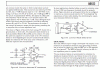
The gain of the AMP04 IC is set using a single external resistor. Therefore, I can switch it back and forth by using digital potentiometer IC controlled by the PIC. Not sure yet which specific chip I’ll use. Suggestions are welcome.

For the 2 ranges:

0 – 50 lbs

IA input = 0 – 45 mV
IA output ≈ 0 – 5VDC
Gain ≈ 111
ADC VREF+ = VDD = 5V
ADC VREF- = VSS = 0V

0 – 5 lbs

IA input = 0 – 4.5 mV
IA output ≈ 0 – 2.5 VDC
Gain ≈ 555
ADC VREF+ = VDD/2 = 2.5V (obtained from the comparator voltage reference module)
ADC VREF- = VSS = 0V

So here are my questions:

  1. Is there anything wrong with using the comparator reference voltage module for the ADC VREF+ input? I didn’t seem to find anything in the data sheet that indicated this would cause problems.

  2. Should I buffer the output of the reference voltage module before feeding it back into the ADC VREF+ pin?

  3. Does anyone have any better ideas for how to go about doing this?

Thanks again for the help. I welcome any and all comments/suggestions. Please let me know if I need to supply any additional information.

Load Cell Datasheet

AMP04 Datasheet

PIC 18F4620 Datasheet
 
hi,
That L/C is rated at 3mV/V with a 10Vdc excitation, so thats 30mV at max rated load.

For the 0-5lbs range, use a rail to rail OPA after the IA opa.
Set the required coarse gain on the IA and use the rail to rail opa for the extra gain.

With regard to using a 10Vdc excitation voltage with a +Vref input the PIC, derive the Vref from that 10Vext, recall that the PIC' adc is ratio metric.
 
Eric,

Thanks for your help and sorry for my slow response. I was on travel over the weekend.

Anyway, I have a few comments/questions about your reply.

That L/C is rated at 3mV/V with a 10Vdc excitation, so thats 30mV at max rated load.

The recommended excitation is 10V but the max is 20V. I was planning to use 15V just to achieve as large a range as possible before the IA stage. For a 0 - 30mV input, 0 - 5V output, and the 0 - 50 lb range, my IA would need a gain ≈ 167 which is still well within the 1 - 1000 range the IA is capable of. The problem comes up in the 0-5 lb range where I'd need a gain ≈ 1667. However, I like your suggestion of having a second OPA to amplify the output of the first IA when working in the 0-5 lb range. Now that I'm going that route, I think I can get away with bringing the excitation voltage of the L/C back down to the recommended 10V.


For the 0-5lbs range, use a rail to rail OPA after the IA opa.
Set the required coarse gain on the IA and use the rail to rail opa for the extra gain.

Do you have any recommendations on an OPA to use for the 0-5lb range? I couldn't find anywhere in the AMP04 datasheet where it said it's a rail to rail IA. I'm also unsure if I should use the same type of amplifier for the second stage or not. Would that be overkill? Cause problems? Any other undesirable effects? For instances when the datasheet does not specifically state "rail to rail", what parameters should I be looking at to tell me if a particular component is or is not rail to rail?


With regard to using a 10Vdc excitation voltage with a +Vref input the PIC, derive the Vref from that 10Vext, recall that the PIC' adc is ratio metric.

I'm a little confused by this comment.

I was planning on supplying the L/C and IA with a higher voltage (originally 15V but now 10V) and then adjusting the gain and offset of the IA so the output range was only 0 - 5V for 0 - 50 lbs and 0 - 2.5V for 0 - 5lbs. I would then switch the VREF+ in software when the user selected each range.

My understanding of how the VREF+ and the VREF- works is that the PICs 10-bit ADC will divide the difference of those 2 voltages by 1024.

So in the 0 - 50 lb case:

ADC VREF+ = VDD = 5V
ADC VREF- = VSS = 0V

(5 - 0)/1024 ≈ 4.88 mV/bit

And in the 0 - 5lb case:

ADC VREF+ = VDD/2 = 2.5V
ADC VREF- = VSS = 0V

(2.5 - 0)/1024 ≈ 2.44 mV/bit

I'm trying to maintain the same 10-bit resolution for both ranges of input voltages.

Am I incorrect about how the VREF+ and VREF- work or am I just missing the point entirely?

Once I get these last questions hashed out, I'm going to start laying out the circuit and when it's done, I'll post it back to this thread for feedback.

Thanks again for the help!
 
hi,
Understood about the Vext part of your post OK.

The OPA after the IA will be a 'normal' OPA, not a IA, it doesn't have to be because the IA has only one output.

I use the MCP6002 dual 5.5V single supply R2R opa.

With reference to part 3 of your post.
When using the internal Vref of the PIC, any small change in +Vs to the PIC, doesn't cause a problem with the adc conversion because the +Vs and the internal Vref are ratio metric, that is they change at the same rate, so the adc conversion remains accurate.

If for some reason the external Vref or the PIC's changed relative to each other, then the adc will not be accurate.

I try to set my OPA gains so that the adc input is +4.887V max, which represents 1000 counts of the adc, this makes the maths a lot easier.

Hope this explanation is OK, if not ask.
 
Last edited:
The OPA after the IA will be a 'normal' OPA, not a IA, it doesn't have to be because the IA has only one output.

I use the MCP6002 dual 5.5V single supply R2R opa.

I didn't know that by definition an IA was a differential amplifier but I understand now. I will look into the MCP6002.

hi,
With reference to part 3 of your post.
When using the internal Vref of the PIC, any small change in +Vs to the PIC, doesn't cause a problem with the adc conversion because the +Vs and the internal Vref are ratio metric, that is they change at the same rate, so the adc conversion remains accurate.

If for some reason the external Vref or the PIC's changed relative to each other, then the adc will not be accurate.

I try to set my OPA gains so that the adc input is +4.887V max, which represents 1000 counts of the adc, this makes the maths a lot easier.

Hope this explanation is OK, if not ask.

I understand now what you meant with the ratiometric comment. However, if the external reference voltage is coming directly from the PIC's onboard comparator voltage reference module, I should be OK because that would change ratiometrically too, right? From the datasheet, I didn't see a way to internally connect the reference voltage output to the VREF+ input (looks like only the VREF- is an option for internal connection) but I should be able to just run a short trace between the 2 pins. The data sheet shows the output being buffered for external connections but I'm not sure if that applies when I'm just going to connect it right back to the PIC. Thoughts?
 
hi,
For the +Vref pin, if you assign the pin as +Vref then the PIC would expect an external voltage as the Vref.
Example, if you used a TL431in its basic configuration for +2.5V, this would connect to +Vref in.
Assuming that the 18F4620 was powered from 5.0V, this would mean that for a adc +2.5Vin signal the conversion would be 1023.

Another way to supply the +2.5Vref pin would be two precision resistors across the the PIC's +5Vsupply.

The 10Vdc to the bridge should also be regulated.
 
For the +Vref pin, if you assign the pin as +Vref then the PIC would expect an external voltage as the Vref.

I guess I still don't understand why I couldn't just connect the comparator voltage reference output to the VREF+ input? For the 18F4620 once all the special function registers were properly set, that would mean jumping RA2 to RA3. Unless I missed something and the PIC can't use the ADC function and comparator voltage reference module simultaneously, I don't understand why that wouldn't work. Am I off base?
 
I guess I still don't understand why I couldn't just connect the comparator voltage reference output to the VREF+ input? For the 18F4620 once all the special function registers were properly set, that would mean jumping RA2 to RA3. Unless I missed something and the PIC can't use the ADC function and comparator voltage reference module simultaneously, I don't understand why that wouldn't work. Am I off base?

hi,
On that PIC I see that you could use the CVRCON register for Vref.OK.
 
Hello again. I finally got around to laying everything out. I tried to visually split up the different parts of the circuit to make the schematic easier to review. Let me know if it helps.

I have a few questions which I grouped according to the different parts of the circuit they relate to. Here they are:

Power Supply:

  • This circuit will be battery powered. Right now I’m thinking 2 AAA or AA batteries. I will need 10V, 5V, and 3.3V sources from those 2 batteries. There is a DC-DC boost converter that I have used before to supply 11-12V. Then there are 3 separate voltage regulators. Is there a better, simpler, or more efficient way to do this? Any thoughts or suggestions?

Load Cell:

  • I'm thinking of adding a cable shield driver like on page 7 of the AMP04 datasheet however, the load cell I'm using only has a common shield for all 4 conductors. How can I modify the diagram in the datasheet to drive a common shield?

1st Stage Amplifier:

  1. What is the purpose of R4 and R5? Are they for impedance matching or something like that? I can't read the values off of this schematic from the thread I linked to in my first post because the resolution is so poor. They are shown as R2 and R3 in that schematic. Are they really necessary? If so, can you recommend a value for them?

  2. The AD8541 buffer for reference voltage is supplied with 5V even though the AMP04 IC is supplied with 10V. I think this is OK because shouldn't the reference voltage be near 0V anyway and therefore should not saturate the AD8541? Can someone please verify this?

2nd Stage Amplifier:

  • I used the extra op amp in the MCP6002 to buffer the offset adjustment similarly to how it's done for the first stage amplifier. Is this good, bad, or even necessary?

Xbee:

  • The Xbee runs on 3.3V but I need the PIC to run at 5V. I accomplish the level change by using a voltage divider. It is shown in the schematic at the far right as R12 and R13. Is the voltage divider a good way to knock the 5V down to 3.3V? On the RX side, I'm directly connected in the Xbee to the PIC because 3.3V is above logical H. Is this OK?

Miscellaneous:

  • Should I separate the analog and digital grounds? I have never done this before but did a little reading. I read somewhere that they can be tied together by a small cap or low value resistor. How do I know if this is necessary and how should I go about doing it if it is?


As always, thanks in advance for your help and advice.
 

Attachments

  • Force Sensor Schematic.PNG
    Force Sensor Schematic.PNG
    210.1 KB · Views: 359
Last edited:
I will tell you where I see what could be a few problems. You are starting with a few AAA batteries into a boost. Then you have 3 regulators. I think, less details your batteries will be short lived. Also remember the 10 volt ref for your bridge is critical to assure accuracy of the bridge, it must be very stable.

Ron
 
I would use a precision 10V reference, and then derive the ADC reference voltage from that using a precision voltage divider, followed by a voltage follower opamp. You must have the ADC reference tracking the bridge excitation voltage.
 
hi vne,
MikeMl has raised the same concern I referred too in my post #2.
The L/C excitation voltage must be stable and ideally the Vref derived from it.

I also agree with Ron, AAA batteries are going to give you grief, a 12V SLA battery say 2 or 5 Ahr would be my choice.
 
Thanks for the suggestions everyone. I'll make some mods and post the updated schematic when I'm done.
 
I'm looking around for a precision voltage reference and most of the ones I found that seemed suitable could only source around 30 mA. The load cell resistance is 385Ω. So that's about 26 mA at 10V. I usually don't like to design that close to a max rating. I did find a lot of precision shunt regulators that can source more current. Can I use one of those? Also, should I power the amplifier with the same precision 10V?
 
I'm looking around for a precision voltage reference and most of the ones I found that seemed suitable could only source around 30 mA. The load cell resistance is 385Ω. So that's about 26 mA at 10V. I usually don't like to design that close to a max rating. I did find a lot of precision shunt regulators that can source more current. Can I use one of those? Also, should I power the amplifier with the same precision 10V?

hi vne,
As you are using a 10 bit adc, to measure 0 to 50lbs, thats approx 50/1000 per bit which is +/-0.05lb for the LSB [0.8oz] I would suggest that you power the whole project from a regulated +5Vdc supply.
So thats the bridge, PIC etc,,, and use the PIC's internal reference Vref.

I understand that the bridge will only give 1.5mV/V when excited by 5V, [ 7.5mV FSD] but all you have to do is increase the IA gain to approx 333 and follow that with a MCP6002 set as a non inverting stage to give a gain of 2, this will give 5V at 50lbs.

For the 0 to 5lbs range use a second MCP6002 with a non inverting gain of 20, after the IA [ which is set for 333], again this will give an overall gain of 6660.
So, 6660 * 0.75mV = 5V to the adc.

Also instead of switching the gains of the IA to suit the 50lbs/5lbs ranges, which could cause problems with any offset voltage you may need, use two separate adc inputs on your PIC.
One for the 50lbs range and one for the 5lbs range.
When used at 50lbs, the 5lbs amp will limit at just under 5V output so it will not cause a problem within the PIC.

Do you follow OK.?
 
Last edited:
Hello again. I’ve tried to incorporate everyone’s suggestions as best as I could and made some changes. I’ve also been doing a fair amount of reading on my own while trying to refine the design. I’d appreciate everyone’s feedback on the latest revision.

First off, I agree with the short battery life comment. Unfortunately, this device will be hand held and relatively small so I’m more or less confined to use cells like AA or AAAs. However, it will only be used intermittently (maybe once a week for 5-10 minutes at a time) so I think I’ll be OK at least for now. Despite that, I took Eric’s advice to ditch the 10V part of the circuit and power everything off of 5V. That should increase the battery life somewhat.

Here are the main changes:

For the power supply portion of the circuit, I lowered the output of the DC-DC converter to 7V. That 7V feeds a MAX6143 precision voltage reference which I’m using as the supply for the analog portion of the circuit. It’s capable of supplying 30mA which I hope will be enough.

The bridge in the load cell will draw about 13mA and all the other analog ICs have operating currents in the µA and nA range. The only other parts that will consume current (aside from leakage) are the shield driver and the PIC's ADC. I’ve tried to find out how much current the PIC's ADC will draw but couldn’t figure it out. Does anyone know the answer to this? Also, how can I estimate the current it will take to drive the cable shield?

Last but not least, I also have the precision 5V output connected to the PICs ADC VREF+ and I’m going to tie the VREF- directly to ground close to the analog portion of the circuit.

For the digital portion of the circuit I’m using the KF50B LDO 5V regulator. Nothing really special there.

In the 1st stage amplifier I made a bunch of changes. First off, I’m now using the INA118 IA IC. The gain is set by VR3 and with an end to end value of 500Ω, the gain should be adjustable from about 10²-10. I’m only going to need 330 or so.

Also, I’m using an OPA602 precision amplifier to drive the cable shield. I got the idea from figure 7 on page 10 of the INA114 data sheet. I was unsure what to do with the "OFFSET TRIM" pins of the OPA602. Should I connect one to supply and one to ground, or just ground both of them? The figure from the INA114 datasheet doesn't mention it and I couldn't really find any useful info in the OPA602's datasheet either.

A few more questions:

  1. Since for the most part I just copied the design, I’m still a little fuzzy on the purpose of a few components in the 1st stage amplifier. I believe R4 and R5 are used to form a low pass filter in conjunction with C16 and C17. Can someone verify this? If my thoughts are correct, then I can go about choosing appropriate values for them.

  2. I believe R2, VR1 and C15 are for offset voltage adjustment. Can someone please verify this too? Or correct me if I’m wrong. If it is for offset voltage adjustment, why is that necessary when there's a dedicated REF pin on the IC? Isn't that what the REF pin is for?

  3. What are the purpose of the inductors L2 and L3? Noise suppression? Are they going to impact the function of the cable shield driver?

  4. Lastly, please help me if you know by telling me how much current draw I can expect from the ADC and shield driver and also what to do with the OPA602’s "OFFSET TRIM" pins.

Thanks again everyone for your help. I know this is a tall order but the design is really coming together. I think pretty soon I’ll be able to order some parts and build a test circuit.
 

Attachments

  • Force_Sensor_V2.PNG
    Force_Sensor_V2.PNG
    262.3 KB · Views: 344
hi vne.

A few more questions:

Since for the most part I just copied the design, I’m still a little fuzzy on the purpose of a few components in the 1st stage amplifier. I believe R4 and R5 are used to form a low pass filter in conjunction with C16 and C17. Can someone verify this? If my thoughts are correct, then I can go about choosing appropriate values for them.

Look at the vne_filter image for an explanation.

I believe R2, VR1 and C15 are for offset voltage adjustment. Can someone please verify this too? Or correct me if I’m wrong. If it is for offset voltage adjustment, why is that necessary when there's a dedicated REF pin on the IC? Isn't that what the REF pin is for?

If the bridge has a offset error, many have, in the order of a mV or so, this is mainly due to any fixtures to the bridge mounting assembly. eg: top plate/ base plate upon which the load being weighed is placed.

When calibrating the scale you will find that the 'slope' of the voltage output of the IA will 'pivot' about this offset point.
So when you set the CAL at full scale weight, you find that the ZERO point has moved.
This means you have to re-zero the scale and redo the FSD CAL again and so on!
Using the VR1 pot 'injects' a mV signal which cancels the signal due to the offset error, so the 'slope' of the IA output pivots about the 'true' zero point.
This makes the CAL easier as the ZERO should be much more stable

The REF on the IA will ONLY move the slope laterally up and down, it will not move the pivot point

What are the purpose of the inductors L2 and L3? Noise suppression? Are they going to impact the function of the cable shield driver?

Again the inductors are for 'noise' filtering.

Lastly, please help me if you know by telling me how much current draw I can expect from the ADC and shield driver and also what to do with the OPA602’s "OFFSET TRIM" pins.

Look at the vne_trim image for the use of the OP602 trim pins.
How long is the cable from the bridge to the IA pcb.???

The shield drivers are usually added for long cable runs.
 

Attachments

  • vne_filter.gif
    vne_filter.gif
    96.8 KB · Views: 335
  • vne_trim.gif
    vne_trim.gif
    14.8 KB · Views: 269
Last edited:
Eric,

Great info! The data sheet for the AD623 seems to verify that R4 and R5 are part of a low pass filter. So, that takes care of questions #1 in my previous post. Also, I think I may be switching up my IA again to the AD623. It does have a slightly higher input offset voltage but appears almost as good as the AMP04 and INA118 and it's the cost. Plus, the data sheet looks pretty informative.

In answer to your question, the cable length from load cell to PCB is 20 feet. My current plan is to just coil the cable into the enclosure. At first I wanted to trim it but then I read somewhere that you should never cut the cable to a load cell. If I remember correctly, the temperature compensation of the load cell is done for a specific cable length. So, if I cut the cable, I'll destroy the temperature compensation. I'm not sure how much this would affect the accuracy as it will be used indoors within a relatively small temperature range. It would make my job a lot easier if I could just cut it. Right now I'm not even sure if all that cable will even fit into the enclosure.

I'm thinking that the wires in the cable have their own resistance, capacitance, etc and if I cut it, I'll change all that to the detriment of accuracy. Although I'm not sure why I couldn't just cut the cable, measure these properties, and then place some components at the inputs of the PCB to mimic as closely as possible a complete 20 ft cable. I'm planning on contacting the manufacturer soon to ask these questions.

Any thoughts?

Thanks!

EDIT: I didn't even notice that you had answered a bunch of my other questions inside the quoted text. Thanks!
 
Last edited:
hi vne,
Look thru these two pdf's about load cell usage.
 

Attachments

  • load_cell_cabling_wiring.pdf
    80.7 KB · Views: 586
  • load_cell_primer.pdf
    159.5 KB · Views: 306
Status
Not open for further replies.

New Articles From Microcontroller Tips

Back
Top