Electro Tech is an online community (with over 170,000 members) who enjoy talking about and building electronic circuits, projects and gadgets. To participate you need to register. Registration is free. Click here to register now.
Welcome to our site! Electro Tech is an online community (with over 170,000 members) who enjoy talking about and building electronic circuits, projects and gadgets. To participate you need to register. Registration is free. Click here to register now.
I tried your impedance matching circuit on the last FM transmitter simulation I posted that had an output of 282mW.
The impedance matching made no difference.
Hi. If you go back and look, you'll see I used 200 ohms, not 2K, since that's what produced the most output power for the 23mW circuit. In simulation the 27pf cap alone in series with a 75 ohm load is just as effective a match as the 154nH and 10pf matching network, because the impedance difference looking into both combinations is only about 100 ohms.
The matching program assumes a perfect inductor. The Q calculated is the Q of the matching network, a measure of the bandwidth of the network. Your matching network attenuates signals at frequencies above and below 100MHz. The higher the Q, the more those signals are attenuated. Q=3 by default. I didn't enter it. For an "L" matching network, the Q "is what it is" based on the what you enter for the other inputs.
Hi Willen, here's how I would go about figuring the values for the interstage matching networks:
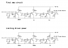
1. The first stage is supposed to deliver 200 mW. For simplicity, I'm going to ignore the few pf of transistor output capacitance. You can tweak the values of the inductor and capacitor, once built. When you build it there are going to be parasitic L's and C's anyway to deal with. The load resistor for 200 mW is RL=V^2/(2P), or 12^2/(2*200mW)=360 ohms. I'm going to also assume an input impedance for the following transistor of 5-5j, which is typical. Using an impedance matching program (because who wants to calculate all that by hand?), the values for L and C of the first matching (diagram B) network between the first and middle stages are 37pf and 75 nH.....
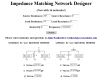
I am still confused on Load Resistance and Source Resistance to fill in Calculator. Can you show another screen shoot of Quoted values here and explain simply between Load Resistance and Source Resistance please!
And what is the purpose of assuming of 5-5j impedance on calculator?
I am still confused on Load Resistance and Source Resistance to fill in Calculator. Can you show another screen shoot of Quoted values here and explain simply between Load Resistance and Source Resistance please!
And what is the purpose of assuming of 5-5j impedance on calculator?
I had to assume something for the input impedance (load impedance), so I chose something typical. The actual value would have to be measured or obtained from the datasheet (if given there). Here is the screenshot. The value for the inductor is different from what I originally posted. Maybe I made a typo.
You mean you have corrected now (Original post has 75nH, 37 pf for 200mw between first and 2nd stage) Now it's 59nH and 37 pf.
Your 5-5j assume impedance is Load Resistance= 5 on calculator?
If this network has 360 ohms impedance as source (output), then this 360 ohms will be as an input impedance for 2nd network but why not? (because collector of Class C has no change of impedance i think).
The +5 for the source reactance should be -5, so the inductor value I originally posted is correct afterall.
The collector of the first stage will see a 360 ohm load with the matching network connected and a 5-5j ohms load on the matching network from the next stage transistor. In other words, the matching network transforms the 5-j5 input impedance to 360 ohms for use by the collector of the first stage.
This site uses cookies to help personalise content, tailor your experience and to keep you logged in if you register.
By continuing to use this site, you are consenting to our use of cookies.

")