Continue to Site

Welcome to our site!

Electro Tech is an online community (with over 170,000 members) who enjoy talking about and building electronic circuits, projects and gadgets. To participate you need to register. Registration is free. Click here to register now.

  • Welcome to our site! Electro Tech is an online community (with over 170,000 members) who enjoy talking about and building electronic circuits, projects and gadgets. To participate you need to register. Registration is free. Click here to register now.

Impedance matching block design

Status
Not open for further replies.

avenue17

New Member
Hi everyone,
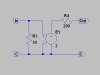
For the lab final project we are required to design a impedance matching circuitry. By the way, the project comes from laboratory of analog electronics course. In this project we will design a circuit which is connected between two adjacent blocks and dynamically matches the input and output impedance of these individual blocks. I have uploaded diagram.
Requirements:

1) The designed circuit shouldn’t disturb the gain, i.e. A=1.
2) The circuit should match the impedance between 30Ω and 200Ω.
3) The circuit gain must vary in a maximum of 0.05, i.e. A=1±0.05.
4) The circuit should be capable of retaining these specifications between frequencies of 1MHz to 5MHz.

my idea:
As we have learned amplifiers for unity gain common collector amplifier should be used for matching impedance.
We have learned how to match a single impedance. But we have not learned how to match dynamic one. i.e. when input impedance increases or decreases our matching block should automatically match that impedance

The deadline is 2 days after. Please give your suggestions according to the course content that i wrote below. Because there may be several ways of doing this project. Thanks in advance for your suggestions. You can call me rami :)

General Course Content:

MOSFET and BJT Amplifiers
High and Low Frequency response of amplifiers
Feedback and topologies.
 

Attachments

  • Untitled.png
    Untitled.png
    16.6 KB · Views: 151
  • Untitled.png
    Untitled.png
    11.2 KB · Views: 146
Last edited:
There is a "Homework" forum on this website, which is where this should have been posted. As a retired Professor, my policy is to make suggestions AFTER you post your work so far, not to hand you a ready made solution...

One suggestion: Change your nomenclature. Number the blocks, 1, 2, 3. You are concerned with matching R1out to R2in and matching R2out to R3in. Your nomenclature is confusing.
 
Last edited:
Ok Mike ML , I have uploaded new version of block diagram. I have made a lot research on Google But I have not found any valuable information on dynamic (or auto) impedance matching. All I have found are advanced techniques that is why I have published this article. Your suggestions will not be MADE solutions. I just need a suggestion to start doing this project. I do not know where to start. If I find any good idea I will work on it. As I have mentioned I have 2 days to submit report
 
Last edited:
First question: Does your intermediate stage require power gain? If yes, then you need an active circuit. If No, you can build a passive network using only L and Cs.
 
It is not required to have power gain. All requirements are stated in my post. Can you just give some sample schematic of this circuit. Will it dynamically match the impedance and how? I do not really understand how this is related with analog course content. Can you give some detailed explanation? Thanks.
 
you can build a passive network using only L and Cs.**broken link removed**

You might be able to, but the OP hasn't had the course where they synthesize filter networks. I suspect that the course instructor is looking for a solution that involves what they have already studied.

Ponder this:

I designed a black box X, shown in the simulations below. In the first simulation, it is driven the way the problem was stated, namely the output impedance of the source is 30Ω, and the impedance of the load is 200Ω. To satisfy the design, the input impedance of of X from In to C should be 30Ω (to match the 30Ω source impedance), and the gain from In (node a) to Out (node b) should be 1. The plot shows that V(a) = V(b)= 500mV (they are perfectly superimposed), so X clearly has unity gain for all frequencies from 100kHz to 10MHz (no phase shift, either)

Why is the voltage at V(a) = 500mV when V2=1V? Well, the only way that can happen is if the input impedance of X (from In to C) is 30+j0, which is what the design asked for.

To check the output impedance of X from Out to C, I moved the source to the other end and drove X backwards 9n the second simulation. Note that V(b) is 500mV, proving that the output impedance of X (which is the input impedance when driven this way) has to be 200+j0 for all frequencies of interest. Also note that V(a)=0, so no signal is passing backwards from Out to In.

Ok, so I have shown you a mystery box X which has the right input impedance, the right output impedance, unity gain going from In to Out, and zero signal passing from Out to In.

What is in the box? Hint, no inductors or capacitors
 

Attachments

  • D9a.jpg
    D9a.jpg
    153.8 KB · Views: 133
  • D9b.jpg
    D9b.jpg
    131.5 KB · Views: 138
Hi,

Are you allowed to use an amplifier? That pretty much makes it simple.
 
Hi,

Are you allowed to use an amplifier? That pretty much makes it simple.

That is what I was driving at. Here is the sub-circuit I used in the simulations I posted above.

E1 is an ideal amplifier, infinite input impedance, zero output impedance, Frequency response flat from DC to light, Gain=2. R3 is a resistor to match the source. R4 is a series resistor so that the amplifier output impedance is set to 200Ω. The Gain of two at the amplifier is required to make the overall gain A=1. The E component in Spice is a Voltage-Controlled Voltage-Source, and is used as a prototype amplifier. Now your job is to create a practical circuit that works like this...
 

Attachments

  • D10.jpg
    D10.jpg
    24.4 KB · Views: 141
Last edited:
You might be able to, but the OP hasn't had the course where they synthesize filter networks. I suspect that the course instructor is looking for a solution that involves what they have already studied.

Ponder this:

I designed a black box X, shown in the simulations below. In the first simulation, it is driven the way the problem was stated, namely the output impedance of the source is 30Ω, and the impedance of the load is 200Ω. To satisfy the design, the input impedance of of X from In to C should be 30Ω (to match the 30Ω source impedance), and the gain from In (node a) to Out (node b) should be 1. The plot shows that V(a) = V(b)= 500mV (they are perfectly superimposed), so X clearly has unity gain for all frequencies from 100kHz to 10MHz (no phase shift, either)

Why is the voltage at V(a) = 500mV when V2=1V? Well, the only way that can happen is if the input impedance of X (from In to C) is 30+j0, which is what the design asked for.

To check the output impedance of X from Out to C, I moved the source to the other end and drove X backwards 9n the second simulation. Note that V(b) is 500mV, proving that the output impedance of X (which is the input impedance when driven this way) has to be 200+j0 for all frequencies of interest. Also note that V(a)=0, so no signal is passing backwards from Out to In.

Ok, so I have shown you a mystery box X which has the right input impedance, the right output impedance, unity gain going from In to Out, and zero signal passing from Out to In.

What is in the box? Hint, no inductors or capacitors

Mike, this was a response to a spammer :D
 
Mike, this was a response to a spammer :D

No, he just wanted a quick answer, and I strung him out... Oh well, maybe someone else can learn from this thread....:rolleyes:
 
No, he just wanted a quick answer, and I strung him out... Oh well, maybe someone else can learn from this thread....:rolleyes:

No, I meant the member you responded to directly to in post #7 :p;)
 
Status
Not open for further replies.

Latest threads

Back
Top