killivolt
Well-Known Member
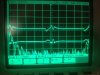
Having issues I'm not sure if it's oscillating or not I've checked all the connections and their ok, maybe to parasitic or something. The GDT is wound correctly. I guess I'll check the I/O next on the GDT.
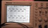
I checked and it's wired correctly, now I just need to check to see if it's oscillating at 30kHz
I checked and it's wired correctly, now I just need to check to see if it's oscillating at 30kHz
Last edited:

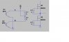
") It shows the SG3525 arrangement for 2 Mosfets driven directly, I noticed it shows the pull down resistors.
It shows the SG3525 arrangement for 2 Mosfets driven directly, I noticed it shows the pull down resistors.