Continue to Site

Welcome to our site!

Electro Tech is an online community (with over 170,000 members) who enjoy talking about and building electronic circuits, projects and gadgets. To participate you need to register. Registration is free. Click here to register now.

  • Welcome to our site! Electro Tech is an online community (with over 170,000 members) who enjoy talking about and building electronic circuits, projects and gadgets. To participate you need to register. Registration is free. Click here to register now.

How to use Vias in Altium Designer to design PCB?

Status
Not open for further replies.

R_ZH

New Member
Hello everyone,

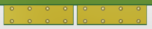
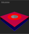
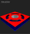
I 'm now designing an adapter PCB using Altium Designer. I want to use some vias to reach the figure in picture 1, but now I always get it like in picture 2. I'm new to PCB design and also new to Altium Designer. I don't know why there is always the space around the vias like in picture 2, which is not possible for manufacturing. Does anybody have ideas how to fix this problem? The attached is my PCB design file. Any help would be appreciated.

Best regards and thanks in advance!
Runze
 

Attachments

  • 1.png
    1.png
    29 KB · Views: 165
  • 2.png
    2.png
    49.9 KB · Views: 176
  • PCB_Project.zip
    50.4 MB · Views: 177
You have to add the vias to the samevl net as the copper areas.
 
It appears the VIAs are not in the same net as the copper area, so are having isolation rings added.

Check the net and try changing it to the same as the main area?

It's not a program I've ever used, but that is a typical different-net effect.
 
Yes, you are right, that's one problem. But after changing it to the same net as the copper area. It became this crossover shape in the picture below. why did it happen like this?
 

Attachments

  • 3.png
    3.png
    50.6 KB · Views: 177
I haven't used Altium, but I suspect you've added a PAD, intended for soldering a component to –:the cross provides thermal isolation from the plane to make soldering easier – instead of a VIA, which won't have thermal isolation.
 
I don't think so. When I double click the component, there will be a column in the properties box showing the Via type and feature. And if that's a Pad, it will show the Pad features. It's different text, I'm pretty sure about that.
 
I'm sorry there seems to be another problem. It really reached the effect in picture 1 in 3D model, but in 2D model if double click the via, it still shows a crossover pattern like in picture 5 and it should actually be the pattern in picture 4. Besides there are no signs of using stitching in picture 4 and it really looks like a normal via. So that maybe not the best way to reach the desired effect. I'm still working on the solutions and any help would also be appreciated.
 

Attachments

  • 4.png
    4.png
    12.4 KB · Views: 167
  • 5.png
    5.png
    14.9 KB · Views: 172
Hello, I found the answer at Design>Rules>Plane>Polygon Connect Style>PolygonConnect. I set the Connect Style to Direct Connect and I got the results I want. And there maybe some distortion to the via connection to Polygon in some layers after resetting, just redraw the polygon and the problem is gone. Yes, you got that idea. It is indeed something related to Thermal Relief box, but we can reset this box using this method. Hope this maybe useful for someone who has the same question.
 
Status
Not open for further replies.

Latest threads

New Articles From Microcontroller Tips

Back
Top