Continue to Site

Welcome to our site!

Electro Tech is an online community (with over 170,000 members) who enjoy talking about and building electronic circuits, projects and gadgets. To participate you need to register. Registration is free. Click here to register now.

  • Welcome to our site! Electro Tech is an online community (with over 170,000 members) who enjoy talking about and building electronic circuits, projects and gadgets. To participate you need to register. Registration is free. Click here to register now.

How does the feedback work in an inverting op amp amplifier?

Status
Not open for further replies.
Your graph should look like this:
 

Attachments

  • opamp gain vs frequency response.png
    opamp gain vs frequency response.png
    14.2 KB · Views: 504
op amp works simply by using as much gain as available to ensure the differential input is zero.

Since the inverting input has two sources the original input and the output via passive components, both must add up to zero or whatever voltage is on (+) side.

The attenuation from the output to (-) is what controls the gain and ends up being just the Z impedance ratio of the -Zfb/Zin(-) or in the simplest case -Rf/Rin
Thank you, Tony.

Those now seem to be very simple principles have been taking me and many experts here a lot of time. Thanks to all of you I've got lots of insights of op amps and much more I didn't obtain in class, I treasure them.
 
Your graph should look like this:
Thank you, audioguru. The graph you provide involves a lot of knowledge inside.

I was trying to prove point 'a' equals to point 'b' in my graph to show that they should look just like the one you gave. Did you have any ideas about how to prove it?
 
Hi,

The open loop or closed loop gain can be calculated for the original simple LT Spice model:

Measured External Open Loop Gain=(Aol*GBW)/sqrt(GBW^2+Aol^2*f^2)

Non Inverting Closed Loop Gain of 1=(Aol*GBW)/sqrt((Aol^2+2*Aol+1)*GBW^2+Aol^2*f^2)

The non inverting closed loop gain is for a voltage follower connection.
To get the gains in db, take the log base 10 and multiply that by 20 (as usual).

Note that the gain of 1 op amp configuration starts out with a gain of 0db at f=0 and ends at -3db at f=GBW.

For a general connection non inverting gain of A we have:
Vout=(Aol*A*GBW)/sqrt((A^2+2*Aol*A+Aol^2)*GBW^2+Aol^2*f^2*A^2)

where A is the circuit gain due to some external resistors, so we get circuit gains such as 1, 5, 10, etc. The external resistors should be greater than 100 ohms, preferably 1k or greater.
Again take the log base 10 and multiply that by 20 to get the gain in db.
 
Last edited:
Hi,

The open loop or closed loop gain can be calculated for the original simple LT Spice model:

Measured External Open Loop Gain=(Aol*GBW)/sqrt(GBW^2+Aol^2*f^2)

Non Inverting Closed Loop Gain of 1=(Aol*GBW)/sqrt((Aol^2+2*Aol+1)*GBW^2+Aol^2*f^2)

The non inverting closed loop gain is for a voltage follower connection.
To get the gains in db, take the log base 10 and multiply that by 20 (as usual).

Note that the gain of 1 op amp configuration starts out with a gain of 0db at f=0 and ends at -3db at f=GBW.

For a general connection non inverting gain of A we have:
Vout=(Aol*A*GBW)/sqrt((A^2+2*Aol*A+Aol^2)*GBW^2+Aol^2*f^2*A^2)

where A is the circuit gain due to some external resistors, so we get circuit gains such as 1, 5, 10, etc. The external resistors should be greater than 100 ohms, preferably 1k or greater.
Again take the log base 10 and multiply that by 20 to get the gain in db.
Thank you very much, MrAl. I have repeated all the calculations of the three gains for open-loop, voltage follower and the general non-inverting configuration, I'm glad I have the same expressions as yours. More importantly, when I substitute the dc gain of the follower or the non-inverting into the open-loop gain expression to find the corresponding frequency, the frequency happens to be the -3dB bandwidth of corresponding configuration! That gives a direct proof of what crutschow said and the graph audioguru gave in post #141, at least a proof for those two configurations.
If you draw a horizontal line at a particular closed-loop gain, then where it intercepts the open-loop plot is the circuit bandwidth at that gain.
 
Thank you very much, MrAl. I have repeated all the calculations of the three gains for open-loop, voltage follower and the general non-inverting configuration, I'm glad I have the same expressions as yours. More importantly, when I substitute the dc gain of the follower or the non-inverting into the open-loop gain expression to find the corresponding frequency, the frequency happens to be the -3dB bandwidth of corresponding configuration! That gives a direct proof of what crutschow said and the graph audioguru gave in post #141, at least a proof for those two configurations.

Hi again,

I am happy to hear that you got the equations to match which shows that you're getting good at this. Writing the equations helps to evaluate these kinds of circuits so you can get a better feel for how they work and see right away how the variables affect the outcomes. This is often more valuable than using a simulator, although the value of a a simulator can not be underestimated either for more direct calculations.

Another thing to keep in mind is that many of the plots are done with either semi log or log log coordinates. The graphs look very different when done with linear coordinates.
 
Hi,

Here is a quick plot of the op amp with three different gain settings (with external resistors) using the equation with the gain factor in it. In this diagram G represents the gain setting with the external resistors.

Noteworthy is that the DC gain for an external gain setting of 100000 does not make it all the way to 100db because the internal gain stage has a gain of only 1e5. With a gain of 1e6 it would come closer.
 

Attachments

  • OpAmpGainWithFrequency-1.gif
    OpAmpGainWithFrequency-1.gif
    11.9 KB · Views: 332
Last edited:
Hi,

Here is a quick plot of the op amp with three different gain settings (with external resistors) using the equation with the gain factor in it. In this diagram G represents the gain setting with the external resistors.

Noteworthy is that the DC gain for an external gain setting of 100000 does not make it all the way to 100db because the internal gain stage has a gain of only 1e5. With a gain of 1e6 it would come closer.
This time, I consider the inverting configuration:
upload_2015-3-12_3-21-10.png

If the input voltage is set to 1 volt with zero phase angle, I calculate the output to be
Vout=( R-R2*Aol)/[(R1+R2)*R*C*s + R+R1+R2+R1*Aol] ---(1) edit:has been corrected

If (R1+R2) is much larger than the capacitor impedance, the output can be approximated as
Vout=-(R2*Aol)/[(R1+R2)*R*C*s+R1+R2+R1*Aol] ---(2)

If I set R=1 then (1) and (2) are about the same and take the value of (2) as the circuit gain of the inverting configuration.

The circuit's dc gain is
dc gain=R2*Aol/(R1+R2+R1*Aol) = A*Aol/(1+A+Aol) ---(3)
in which A=R2/R1 is the circuit's external gain.

Aol=1e5,
When A=1, dc gain=~ 1=0dB.
When A=100, dc gain=~ 99.899=39.99dB
When A=100000, dc gain=~ 50000=93.98dB
When A=100000, Aol=1e6, dc gain=~ 90909=99.17dB
upload_2015-3-12_4-24-54.png

But it's strange that when the external gain equals unity, the curve at high frequencies doesn't intersect with the other two, and it also doesn't intersect with the op amp's open-loop gain curve. Hmm ...
upload_2015-3-12_5-11-4.png


Now let's go back to equation (2).
It can be rewritten to see that the circuit's bandwidth is
BW=GBW*(1+A+Aol)/[(1+A)*Aol]

The gain bandwidth product is the product of the dc gain (3) and BW:
[A/(1+A)]*GBW
which equals to a constant GBW only when the external gain (R2/R1) is much larger than unity.

So it seems to be that in addition to having to have a large open-loop gain, in this inverting case the ratio R2/R1 also has to be large for the circuit to have a behavior we expect.(?)
 

Attachments

  • upload_2015-3-11_15-48-16.png
    upload_2015-3-11_15-48-16.png
    44.4 KB · Views: 297
  • upload_2015-3-12_5-10-7.png
    upload_2015-3-12_5-10-7.png
    52.6 KB · Views: 328
Last edited:
Hello again,

Well if we factor the -3db down frequency point we get:
fcutoff=GBW*(G/Aol+1/Aol+1)/(G+1)

and we can immediately see that when Aol is large and G much lower, this approximates to:
fcutoff=GBW/(G+1)

and we can see that for low G, G becomes comparable to that "1" in the denominator, so we end up with a lower frequency because that '1' is not insignificant.

G is the external circuit gain set with the two external resistors.

The physical reason for this might be because the error voltage at the inverting terminal is lower than what it is with a non inverting configuration so that the internal gain is not as effective with a gain of 1. In the non inverting config, the output connects directly to the inverting input so there's no divider action. We could look into this more...you could look at the inverting terminal error voltage and see what you can spot...in other words, find out what causes that extra gain loss at a gain of 1 or 2.

See attached plots for gains of 100000, 100, 10, 5, 2, and 1.
 

Attachments

  • OpAmpInvertingGainWithFrequency-1.gif
    OpAmpInvertingGainWithFrequency-1.gif
    10.1 KB · Views: 327
I just want to congratulate all the posters in this thread. This has got to be one of the best threads I've seen in a homework section, and I mean crossed all the forums I've visited in the last 20 years.. Keep up the good work Heidi, as you epitomize what a good student does with a resource like this. I can tell you've learned a lot from this thread and I've enjoyed seeing your growth. I can see you paying this forward as time goes on.

Congrats everyone. Keep up the good work.
 
Thanks, JoeJester. Thanks to all the experts helping me, I did learn a lot which I didn't obtain in class.

Thanks again!
 
Well if we factor the -3db down frequency point we get:
fcutoff=GBW*(G/Aol+1/Aol+1)/(G+1)

and we can immediately see that when Aol is large and G much lower, this approximates to:
fcutoff=GBW/(G+1)

and we can see that for low G, G becomes comparable to that "1" in the denominator, so we end up with a lower frequency because that '1' is not insignificant.

G is the external circuit gain set with the two external resistors.
Thank you, MrAl.

Here's how I understand your explanation:
From equation (3) in post #149, the dc gain is
(R2/R1)*Aol/[1+(R2/R1)+Aol]
or
G*Aol/(1+G+Aol)

If G is low, for example, G=1, and Aol is large, then the dc gain of the inverting amplifier will be approximately 1. If we look at the op amp's open-loop gain plot in #149, when the inverting amplifier's dc gain is one, we expect its cutoff frequency should be GBW, but in fact the cutoff frequency for G=1 is approximately GBW/(1+G)=(1/2)*GBW.
The physical reason for this might be because the error voltage at the inverting terminal is lower than what it is with a non inverting configuration so that the internal gain is not as effective with a gain of 1. In the non inverting config, the output connects directly to the inverting input so there's no divider action. We could look into this more...you could look at the inverting terminal error voltage and see what you can spot...in other words, find out what causes that extra gain loss at a gain of 1 or 2.
If I want to evaluate the inverting amplifier's frequency relationship with output voltage Vout, the inverting terminal voltage Vn, the circuit's gain or its cutoff frequency, taking the internal R and C into consideration, I use the following circuit and superposition, that's all I know. How do you define the 'error voltage'?
upload_2015-3-13_23-14-40.png
 
Last edited:
I just want to congratulate all the posters in this thread. This has got to be one of the best threads I've seen in a homework section, and I mean crossed all the forums I've visited in the last 20 years.. Keep up the good work Heidi, as you epitomize what a good student does with a resource like this. I can tell you've learned a lot from this thread and I've enjoyed seeing your growth. I can see you paying this forward as time goes on.

Congrats everyone. Keep up the good work.

Hi Joe,

I have to agree 100 percent, as Heidi followed this thread like clockwork and found ways to solve the problems that came up. That shows true progress and it makes me feel very good to see that i helped in at least some small way. It's certainly not every day you see the kind of interest and dedication that Heidi has shown and i am happy to see that she takes the time to figure all this stuff out.
 
Thanks, JoeJester. Thanks to all the experts helping me, I did learn a lot which I didn't obtain in class.

Thanks again!

Hi there Heidi,

A lot of us here had to do this kind of stuff for a living at one time, and in that kind of setting failure is not an option. You either solve problems or starve :)

If you look back at the newest graphs i posted, I was suggesting that you try to find out why the actual gain drops off a little faster than expected once we get past a gain of maybe 5. I posted plots for set gains of 10, 5, 2, and 1, so we could all observe the decrease that seems to start under 5, noting especially gains of 2 and 1.

One way would be to look at the 'error' voltage, but also at the output voltage and the internal gain Aol, to see how they play against each other at frequencies say under 10 Hz. In control theory it is called the 'error' voltage because it is what gives the amplifier the ability to 'correct' the output voltage to what it is supposed to be relative to what it actually is at the time, on a nano second to nano second time basis. That is, if we look at the behavior over time we see the output voltage become closer and closer to the correct output for what the input voltage has initiated when it was first applied. As you know, it takes time to get the right output for any given constant input (the sine is considered constant on a pseudo instantaneous basis too). But interestingly, even when the exponentials have all died down (with possible sine components still remaining), there still remains some error voltage and that is what drives the Aol gain into making the output what it is, along with any filtering action of the RC network.

For an op amp, the error voltage is simply the difference between vp (non inverting input) and vn (inverting input), so it is just (vp-vn) and because we are using vp=0 in these circuits that means the error voltage is just -vn or looking at the absolute value just vn.

So what i would suggest is that for a given input like 1v, you calculate the output voltage, vn voltage, and the voltage at the output of the internal gain stage Aol before the RC filter, and see what you can find out. Note that because we are dealing with AC signals you may have to include the phase shift of each node too, probably with respect to Vin's phase which we can consider to be zero.
The most likely frequencies to look at would be 5 Hz and below, or something like that, because that is where the discrepancy begins to show itself.

So far, because of the discrepancy, we cant be sure if we have the right results or we made a bad assumption somewhere. In real life, we'd like to be sure one way or the other so we keep looking until we find the answer :)
 
Like we have many elderly people here in Taiwan, they help direct traffic when school children are going to and leaving from school. They dedicate their time and energy to the service and certainly they deserve a little (compared to what they're giving) feedback for their living. They earn people's respect. I appreciate all your work here.

As for the circuit behaviors, I always want to redo the analysis like you did in post #47. I believe everything will be clearer and clearer!
 
Last edited:
So what i would suggest is that for a given input like 1v, you calculate the output voltage, vn voltage, and the voltage at the output of the internal gain stage Aol before the RC filter, and see what you can find out. Note that because we are dealing with AC signals you may have to include the phase shift of each node too, probably with respect to Vin's phase which we can consider to be zero.
The most likely frequencies to look at would be 5 Hz and below, or something like that, because that is where the discrepancy begins to show itself.
Hello MrAl,

I do some calculation for the inverting amplifier's steady state response, it seems that for the imaginary model in Fig.1 below, the results approximate to that of the ideal model 'opamp' in LTspice. Do I misunderstand what you want me to look at?

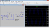
For the following inverting amplifier in Fig.1, assume that the resistance (R1+R2) is much larger than the impedance of the capacitor and the parallel impedance of R and C. I derive some expressions for steady state response in which Vin, Vout, vn and vo are in phasor forms.
upload_2015-3-16_19-21-9.png

Voltage transfer function:
Vout(s)/Vin(s) = -G*Aol/[(1+G)*R*C*s+1+G+Aol]
= -[G*Aol/(1+G+Aol)]/{1+jf/[(1+G+Aol)/(1+G)(Aol/GBW)]} ---(1)
where G=R2/R1, Aol is the VCVS's gain or the op amp's open-loop gain, f is the input voltage's frequency in Hz.

From which the amplifier's dc gain is
dc gain = G*Aol/(1+G+Aol) ----(2)

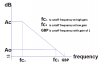
The inverting amplifier's 3-dB frequency is
fcutoff = (1+G+Aol)/[(1+G)(2*pi*R*C)] = GBW*(1+G+Aol)/[(1+G)*Aol] ---(3)

The inverting terminal voltage vn is
vn = (1+jf*Aol/GBW)*(G*Vin)/[1+G+Aol + jf*(1+G)*(Aol/GBW)] ---(4)

I define A(s) as such that (vp-vn)*Aol*A(s)=Vout,
A(s) = (1/s*C)/[R+1/(s*C)] = 1/(1+jf*Aol/GBW) ---(5)

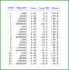
For Vin=1V, Aol=100k, GBW=1meg Hz, G=R2/R1=1k/1k=1, f=1Hz,Vout from (1) is
Vout= 0.99998(180 degree)
or in time domain,
Vout(t)= 0.99998*sin(360*t+180), ----(6)
which is consistent with the simulation:
upload_2015-3-16_21-31-5.png


For f=1k,
Vout= 0.999978(180.11459 degrees)
or
Vout(t)= 0.999978*sin(360*1000*time+180.11459):
upload_2015-3-16_22-40-1.png

-----------------
Now let me evaluate Vout through Vout=(vp-vn)*Aol*A(s):
For f=1, G=1, Vin=1, Aol=100k, GBW=1meg, vn from (4) is
vn= 10.04968u(5.71059 degrees) ---(7)
A(s) from (5)
A(1Hz)= 0.995037(-5.71059 degrees)
and Vout= -0.99998(0 degrees)
or
Vout(t)= -0.99998*sin(360*time),
which is equivalent to (6).

From (7),
vn(t)= 10.04968u*sin(360*time+5.71059):
upload_2015-3-17_0-39-37.png
 

Attachments

  • upload_2015-3-16_22-3-45.png
    upload_2015-3-16_22-3-45.png
    44.6 KB · Views: 303
Hello again Heidi,

Well, the idea is to use the model to find out why the measured gain goes down more when we get to a gain of maybe 1, or 2, and see what is actually causing this, other than the purely formulatic math view. So to start looking at all the node voltages with a few different frequencies might help.
Did you find out anything after doing that analysis, anything that helps us understand the reason for the dip in gain for very very low gains like 1 or 2?
A simulator may be enough to discover more about this, using the model we have been talking about.
I am just throwing some ideas out there so you have a starting point, but you may wish to think about how you can understand this better yourself and come up with ideas. The simulation route seems to be the quickest so maybe looking at the signals will lead to some interesting conclusions.

To save you some work i have prepared this chart. It is a chart that shows the actual gain and phase shift for several set gains from 1 to 10.
I do not show frequencies below 1000 Hz because they show about the same results as that at 1000 Hz.
Note that i am posting this because looking at these numbers may reveal why we see a difference at low gains, not because it is definite that this will help. This may help a little, or not at all, or reveal the entire reason.
(See attachment far below for a better chart)

Code:
G      F      Vout    Db    Ph
---  ------  -----   ----  -----
 1      1000   1.00    0.0  179.9
 1     10000   1.00    0.0  178.9
 1    100000   0.98   -0.2  168.7
 1   1000000   0.45   -7.0  116.6
 1  10000000   0.05  -26.0   92.9
 2      1000   2.00    6.0  179.8
 2     10000   2.00    6.0  178.3
 2    100000   1.92    5.6  163.3
 2   1000000   0.63   -4.0  108.4
 2  10000000   0.07  -23.5   91.9
 5      1000   5.00   14.0  179.7
 5     10000   4.99   14.0  176.6
 5    100000   4.29   12.6  149.0
 5   1000000   0.82   -1.7   99.5
 5  10000000   0.08  -21.6   91.0
10      1000  10.00   20.0  179.4
10     10000   9.94   19.9  173.7
10    100000   6.73   16.6  132.3
10   1000000   0.91   -0.9   95.2
10  10000000   0.09  -20.8   90.5

[/FONT]
 

Attachments

  • OpAmpGainPhase-1.gif
    OpAmpGainPhase-1.gif
    17.9 KB · Views: 303
Last edited:
Hello MrAl,

Sorry I didn't see the chart you presented until now. I thought you wanted me to observe the node voltages at low frequencies for G=1 or 2, so I did some calculations using the formulas in post #157, here's the results:
upload_2015-3-19_4-13-21.png

where vn is the voltage of the op amp's inverting terminal calculated by equation (4), op amp's internal gain by [Aol*A(s)] in (5).

The magnitudes (A*B) of the output voltages or the voltage gains of the inverting amplifier didn't vary significantly at these frequencies (but their corresponding dB values may have noticeable differences). However, I can see that once the voltage difference (vp-vn) increases, the op amp's gain must decrease to ensure a constant output.

I repeated the calculations by using formula (1) in #157, I'm glad they closely match yours.
upload_2015-3-19_5-9-51.png

I think that Vout deviates further from expected with increasing frequency for a given G is because of
|Vout| = (G*Aol) / sqrt[(1+G+Aol)^2 + ((1+G)^2)*((Aol/GBW)^2)*f^2],
for Vin=1.
 

Attachments

  • upload_2015-3-19_4-51-1.png
    upload_2015-3-19_4-51-1.png
    20.8 KB · Views: 293
I just saw the underline at 1000000Hz, the gain decreases dramatically, hence we have to raise the Aol to have a larger feedback, or to cause a smaller differential input to increase the output accordingly.(?)
 
Status
Not open for further replies.

Latest threads

Back
Top