Continue to Site

Welcome to our site!

Electro Tech is an online community (with over 170,000 members) who enjoy talking about and building electronic circuits, projects and gadgets. To participate you need to register. Registration is free. Click here to register now.

  • Welcome to our site! Electro Tech is an online community (with over 170,000 members) who enjoy talking about and building electronic circuits, projects and gadgets. To participate you need to register. Registration is free. Click here to register now.

Help Needed: PIC Full Bridge PWM + Bridge Driver not working

Status
Not open for further replies.

Speakerguy

Active Member
Hey guys,

I am working with an 18F4550 and a HIP4082 full bridge driver. I'm decent with PIC's and I have all four PWM outputs working (have probed with scope).

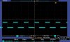
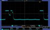
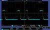
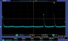
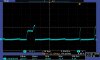
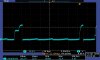
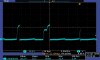
I cannot seem to get the high side gate drive signals working properly coming out of the HIP4082. The low side signals are very good in either direction, but the high sides look like garbage. I would try to describe them to you but I'm not sure what I'm looking at on the scope really. I think my problem is likely with the bootstrap but I've tried multiple diodes and caps to no avail. I've attached my schematic. Have tried Shottky bootstrap diodes as well as regular S1B diodes and 10, 100, and 1000uF caps for the bootstrap sections. Also multiple frequencies from low <10khz to above 100khz.

If someone could look over my schematic and the data sheet for the HIP4082 to see if I did something stupid, I would really appreciate it. Thanks!

HIP4082
https://www.electro-tech-online.com/custompdfs/2009/04/fn3676.pdf
 

Attachments

  • untitled.JPG
    untitled.JPG
    79.4 KB · Views: 4,430
Last edited:
Additional info: All FET's are N-Channel 40V 50A 11mOhm Rds(on). TVS diodes are 24V operating 1.5KW peak dissipation. Schottky's are SK154 15A 40V (very nice). Using positive polarity on all outputs from the PIC. Logic level inputs to the HIP4082 (5V). Please ask if there is anything else you want or need to know, I'm really trying to figure out why my high side gate signals suck.

EDITED TO ADD: Corrected FET info.
 
Last edited:
Can you define 'looks like garbage' a little better?
 
Also what ground are you using for checking the high side gates? You should be grounding the scope at the mosfets source, not the common ground.
 
Last edited:
Here are four single-shots of the signals. First is the low-side gate drive signal (lower left in the schematic). The next three are single-shots of the high-side (top right) with a 100uF cap and a Schottky on the bootstrap.
 

Attachments

  • tek00015.JPG
    tek00015.JPG
    51.6 KB · Views: 780
  • tek00016.JPG
    tek00016.JPG
    51.4 KB · Views: 530
  • tek00017.JPG
    tek00017.JPG
    52.1 KB · Views: 656
  • tek00018.JPG
    tek00018.JPG
    51.1 KB · Views: 514
Last edited:
Also, the other high side driver (top left in schematic) is getting a gate signal like this. It only has a 10uF bootstrap on it (I am playing around with values).
 

Attachments

  • tek00019.JPG
    tek00019.JPG
    51.8 KB · Views: 482
  • tek00020.JPG
    tek00020.JPG
    51.9 KB · Views: 430
  • tek00021.JPG
    tek00021.JPG
    51.7 KB · Views: 423
Also what ground are you using for checking the high side gates? You should be grounding the scope at the mosfets source, not the common ground.

OK, will do. The shots above are all referenced to board ground.
 
Yea, using the common ground will make your high side signals look all kinds of funky, as the signals are also going through the low-side circuitry before getting to ground. The low-side circuitry is causing the strange view of the high-side signals.

Also, what is the part number of the FETs?
 
Well frak me. I had my ICSP connector hooked up while I was messing around with measurements, and managed to short something out (grounded o-scope). I didn't notice it immediately but I saw after a bit that the programming LED wasn't green (normal stand-by state). It was unlit, so I picked up the little plastic case it was in and it was HOT. Took out the board from the case and the PIC was nice and toasty. Thankfully the USB port on my computer didn't go along with it.

Sigh. Well, no programming changes for the next five days til I get a replacement in. Maybe this power electronics stuff is not for me :(
 
Nono, don't want gate drive and source voltage speakerguy.
You need to take the gate reading from the high side fets with a ground refrence from the source, you can't use the system ground for a high side fet. All FET gate voltage readings should ALWAYS be takeing from the source as a ground refrence, because that's how they operate, they could care less what the rest of the circuit is at.
 
Last edited:
I've had limited success with the HIP drivers. I've managed to burn my way through 6 of the drivers and 18 of my collection of IRF540 but mainly down to bad motor connections and my own mistakes lol.

10-100uF on the bootstrap seems rather high. I vaguely remember using 100nF capacitors for the bootstrap and it all working fine.
 
Update - looking at some of my old datasheets the bootstrap capacitor seems to be specced for 100nF to 220nF.
 
Scaedwin,

The last image I posted is of the gate referenced to ground, and the source referenced to ground. So the difference between the two is the Vgs for the high side FET, I just didn't put the scope into math mode and do a difference signal.

picbits,

NOW you tell me about limited success with the HIP drivers :) j/k. I have some 1 and .1uF caps I could try. I just had no idea what size it would take so I started off with 10 as a baseline. I have another board that has everything but the micro populated. I could try that one, but I just blew up my programmer. I think I'm out of business for a few days on this project, but I'll tinker with the hardware some more. Good thing my fish tank needs some attention and I've got some DVD's I need to watch else I'd get bored.
 
I don't understand why people are so averse to P channel fets =\ Then you can just drive them directly.
 
Found what I was looking for ...

On the demo board text it says ....

Consistent with good design practice, the +12V bias supply
is bypassed by capacitors C6 and C5 (at the IC terminals
directly). Capacitor C6 is a 4.7mF tantalum, designed to
bypass the whole PCB, whereas C5 is a 0.22mF, designed to
bypass the HIP4081A. The bootstrap capacitors, C3 and C4,
and the high voltage bus bypass capacitors are 0.1mF, 100V
ceramic. Ceramic is used here because of the low
inductance required of these capacitors in the application.

So they are using 0.1uF capacitors on their demo boards. Might be worth a look. This is for the HIP4080/4081 but the principle is the same.

Page 11 of this datasheet
https://www.electro-tech-online.com/custompdfs/2009/04/an9405.pdf
 
I don't understand why people are so averse to P channel fets =\ Then you can just drive them directly.

N channel have a lot lower Rds On vs $$$/£££ and are easier to get in the high power/lower RDS.

The Intersil drivers also include hardware "dead time" and when they are working are rather nice easy drivers to use for Mosfets.

Even if you used P Channel then you still have to drive their gates with a decent drive circuit for high powered applications to minimise heating effects while the FET is in its linear zone.
 
The "ground" on the high side FETs is not the same as the common ground. It's the source output pin of the FETs themselves. Put the scope probe on the gate pin, and the scope ground connection on the source pin. That will show you a proper gate signal.
 
I tried that, but then my power supply started whining. I guess it is not as isolated as it is supposed to be? (scope is grounded). I got better results with the two probe method. I might as well shell out the cash for a differential probe I guess.

Also I tried with 0.1uF caps, and it didn't work at all. No high side gate signals at all, dead flat. Maybe my schottky's are too leaky?
 
Last edited:
Status
Not open for further replies.

Latest threads

New Articles From Microcontroller Tips

Back
Top