Continue to Site

Welcome to our site!

Electro Tech is an online community (with over 170,000 members) who enjoy talking about and building electronic circuits, projects and gadgets. To participate you need to register. Registration is free. Click here to register now.

  • Welcome to our site! Electro Tech is an online community (with over 170,000 members) who enjoy talking about and building electronic circuits, projects and gadgets. To participate you need to register. Registration is free. Click here to register now.

Help: how to determine the quiescent current/voltage of the circuit (hood)?

Status
Not open for further replies.

xiongyw

New Member
Hi, all,

I am studying Hood 1969/1996 circuit. I read the articles by JLH (1969/1996/2000), but since I am new to electronics, I can not fully understand the descriptions (and assertions) in these articles.

The first step for me seems to understand the quiescent status of the circuit. But after days of gazing on the circuit, I do not have a clue yet.

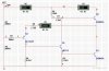
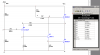
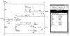
The attached is a simplified circuit without feedback caps/etc, and the simulation shows quiescent current/voltage pretty close to what the circuit is expected to be.

The problem for me is that, I have no idea, using paper/pencil, how to estimate the quiescent current/voltage? Actually I do not know where to start, even assuming all Vbe=0.6 and all beta=100 (e.g.), but every points seems depends on other points (in terms of voltage/current).


It will be very helpful if you can give any hints on this, and/or point out the relevant background information I am missing (so I can go to check related chapters in text books).


Thanks a lot,
/bruin
 

Attachments

  • hood.jpg
    hood.jpg
    146.9 KB · Views: 1,052
Start with assumption that the output (node 1) is half supply. The actual output voltage will be offset to high side by Vbe of Q4 and its emitter resistor feedback to output because base of Q4 is biased at half supply. Node 1 will be about 30.2 vdc. This is both A.C. and D.C. feedback.

Current through both output devices should close to equal with upper output device having more emitter current to supply the Q4 feedback, as their base current. Q3 current is about 22.8 mA. This current is distributed between base drive current on bottom output device and 2.2K. Assume 0.65 vdc Vbe on bottom output device so 0.65v/2.2K = 0.3 mA goes down resistor leaving 22.8 mA - 0.3 mA = 22.5 mA going into bottom output device base. With beta =50 then output current is 22.5 mA * 50 = 1.1 amps which is close the the 0.9 amps of sim. Need to iterate to zero in.

From your sim there seems to be a high quiescent bias current through the output devices. This is not class B operation. Will require one very big heat sink to dissipate 40 watts of heat.
 
Last edited:
Thanks for your reply, RCinFLA!

So it seems the following can be regarded as start points:

- Node 2 is around half Vcc (because of the divider)
- Node 1 is also around half of Vcc (because of two matched output BJTes?). Also node 1 should be higher than node 2, in order for Q4 to be in operation, and this can be done by adjusting the divider (R1 or R2).
- Current through R5 (2.2k) is about Vbe/R5 (0.65v/2.2k).

I am still missing the point on how the current through Q3 is estimated (22.8mA as you mentioned). Can you give more hints?

Also, the sim result about voltages at node 1 is a little bit more than 20vdc (node 2 is about 19.* vdc), not as high as your estimation (30.2vdc, may be it's a typo?). How you get this value?

Another question is how to estimate the maximum swing of the output voltage? e.g., how much the difference between supply voltage and Vout (peak-to-peak) usually be? I guess this determines the maximum power can be delivered to the louder speakers (with a given impedance).

Btw, the AC signal input is at node 3, according to the schematics on the last page of <http://www.tcaas.btinternet.co.uk/jlh2000.pdf>.

Thanks again,
/bruin
 
Last edited:
Analogue circuits are notoriously difficult to analyse especially when there is feedback. This is no exception.

I am surprised you have simulated a current through R8 of 3.553mA. This would imply a voltage drop across R8 of 9.5V. Assuming the emitter of Q4 is roughly 20V, your output quiescent point is sitting 9.5V high.

I think the only thing you can be certain of is that Node 2 is at 20V (assuming the current into the base of Q4 takes little current). Now, with this in mind, if the output rises above 20V (vcc/2) then there will be large voltage drop across R8. This will cause a high current into the emitter of Q4 that will mean a high current into the collector of Q4. This will cause a high voltage across R4 and turn on hard Q3 and Q1. This will bring down Node 1, reducing the voltage across R8, regulating the current in R8.... etc etc as above.

If the output is at 20V, the voltage drop across R8 is minimal as Q4's emitter is at Vcc/2 (give or take a Vbe) minimising the current in R4, switching off Q3 and Q1.

This is the best way (for me) of analysing it. Still cannot understand the current in R8 being 3.553mA:D
 
It is a class-A "heater", not an ordinary class-AB audio amplifier.
It wastes a very high amount of current.
 
Q3 will be less then I first stated because Q2 base is taking some of this current which I did not include in first pass estimate.

Doing an existing circuit with feedback requires iterations. It is much easier to design one from scratch when you know what you want.

Everything flows from the input divided voltage.
 
Last edited:
Hi

I agree with you - the only thing you can be certain of is that the input divider produces vcc/2 (ignoring the load of Q4's base). I suspect that the great Hood did not pick the value of the resistors, just tweaked them to set the bias points impirically. This then puts everyone else at a disadvantage trying to analyse the circuit!

However, I have one of his books in the loft and I am going to dig it out to see if I can design an audio amp as it is one of the most rewarding areas of electronics!:D
 
Thanks for the reply.

Analogue circuits are notoriously difficult to analyse especially when there is feedback. This is no exception.

I am surprised you have simulated a current through R8 of 3.553mA. This would imply a voltage drop across R8 of 9.5V. Assuming the emitter of Q4 is roughly 20V, your output quiescent point is sitting 9.5V high.


I think the only thing you can be certain of is that Node 2 is at 20V (assuming the current into the base of Q4 takes little current). Now, with this in mind, if the output rises above 20V (vcc/2) then there will be large voltage drop across R8. This will cause a high current into the emitter of Q4 that will mean a high current into the collector of Q4. This will cause a high voltage across R4 and turn on hard Q3 and Q1. This will bring down Node 1, reducing the voltage across R8, regulating the current in R8.... etc etc as above.
It seems the voltage accross R4 may not be controlled by the collector current of Q4, since voltage at node 4 equals the Vbe1+Vbe3 (0.81+0.76=1.57, according to sim result), assuming both Vbe does not vary too much in this case. So the increase of Ic4 will mostly flow into Q3's base, which in turn increase Ie3; and similarly, the increase of Ie3 will mostly flow into base of Q1, since the voltage across R5 is also relative constant (0.81, according to sim result). Is this kind of reasoning correct?

If the output is at 20V, the voltage drop across R8 is minimal as Q4's emitter is at Vcc/2 (give or take a Vbe) minimising the current in R4, switching off Q3 and Q1.

This is the best way (for me) of analysing it. Still cannot understand the current in R8 being 3.553mA:D


I enclosed another picture with DC operating point simulated by MultiSim. The current through R8 is much less than 3.553mA, by using (V1-V8)/R8=0.216mA. Strange, may be I was not correctly using the software when it producing 3.553mA...

Based on the DC operating points, I can calcuate the currents flowing in most of the segment, except the base current into Q1 and Q2, plus the collect current of Q3:

- Ie4=(V1-V8)/R8=216u, Ib4=IR3=(V3-V2)/R3=1.4u, so Ic4=Ie4-Ib4=214.6u
- IR5=V4/R4=190u, so Ib3=Ic4-IR4=214.6-190=24.6u
- IR6=IR7=(Vcc-V6)/(R6+R7)=13.2m
- IR5=V5/R5=370u

then I stuck at this point, without knowing how IR7 is splitted at node 6, and then how Ie3 should be...
 

Attachments

  • hood2000_quiescent.PNG
    hood2000_quiescent.PNG
    29.2 KB · Views: 424
Last edited:
Picture with the current calculations, based on sim result.
 

Attachments

  • hood2000_quiescent2.PNG
    hood2000_quiescent2.PNG
    53 KB · Views: 486
I think you are over complicating things and I doubt if JLH went to this much trouble in analysing his circuit.

Your assumptions about the voltage across R4 is correct - it is clamped by the 2Vbes of the transistors. I am not sure if you can say that most of Q4's current flows into Q3 and likewise, Q3's current into Q1, but some of it will at least.

If you want to go with a detailed analysis of the circuit, it might be easier if you break the feedback loop at node 11, connect node 11 to 0V and analyse it from there. With feedback every node changes with every other node and you can end up driving yourself mad:eek:

Thanks for the suggestions. Definitely I do not want to drive myself mad:)
I just don't know how JLH (or other gurus) will analysis the circuit like this. E.g., I saw from somewhere else (by Nelson?) that it has a open loop gain xx, feedback yy, and a close loop gain zz=xx-yy, so I guess they should know how to get this numbers by calculations :)

btw, which node you were really refering to by "node 11", which does not exist on the schematics? It seems it's at least not "node 1", since otherwise Q4 will be shutdown.

Thanks again.
 
It's possible to analyze the circuit and get all the currents and voltages if you set up 17 equations in 17 unknowns. The system can be solved easily with a mathematical assistant program.

I used the Shockley equation for the Vbe-Ie characteristic of the transistors. In order to get a Vbe of about .8 volt for Q1 and Q1, it's necessary to use a saturation current, Is, of 10^-14. I don't think this is realistic. A 2N3055 isn't going to have a Vbe of .8 volts at room temperature with a base current of only 5 milliamps or so.

I've attached 3 images. The first shows Vbe curves for two different saturation currents plus a linear approximation.

The second image shows the network solution with Is chosen so that the Vbe of Q1 and Q2 is about .8 volts. This corresponds with the numbers you got fairly closely.

The third image uses a reduced saturation current for the transistors of 10^-12, which I think may be more realistic.

The designators for currents should be obvious; IC2 = collector current of Q2, IB1 = base current of Q1, etc.

I used different node numbering than you did.

Code:
     My      Your
    node     node
   number   number

     1        2
     2        3
     3        4
     4        8
     5        1
     6        7
     7        6
 

Attachments

  • VbeCurve.png
    VbeCurve.png
    8 KB · Views: 362
  • Quiescent1.png
    Quiescent1.png
    15.3 KB · Views: 375
  • Quiescent2.png
    Quiescent2.png
    15.3 KB · Views: 305
Last edited:
Status
Not open for further replies.

Latest threads

New Articles From Microcontroller Tips

Back
Top