Continue to Site

Welcome to our site!

Electro Tech is an online community (with over 170,000 members) who enjoy talking about and building electronic circuits, projects and gadgets. To participate you need to register. Registration is free. Click here to register now.

  • Welcome to our site! Electro Tech is an online community (with over 170,000 members) who enjoy talking about and building electronic circuits, projects and gadgets. To participate you need to register. Registration is free. Click here to register now.

H-Bridge DC motor driver

Status
Not open for further replies.
MrNobody said:
Thanks for your explanation.. Initially, i do not really understand.. but after searching on the internet, i found MOSFET application note by DALLAS semiconductor.. Now I understand..
When you say "source flowing at about 5 to 10V",
I made a mistake, meant the drain will be floating at 5 to 10V.

do u mean the V(DS) would be 60V - 10V which is 50V..?
Yes, you need to pull the source 10 or so V below the drain before it will switch fully on.

Did i understand correctly..? If that is the case then the power loss would be too much...
Yes, the poor MOSFET will have 50V between the drain and source whilst carying the current.

Can I ask, how to calculate the Voltage at source of MOSFET..? what formula should I use..?
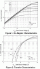
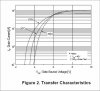
Look at the graph of current vs gate source voltages on the datasheet.

If I use P-MOSFET for high-side driver, the source terminal (of MOSFET) would be connected to the 60V and the drain would be connected to the motor rite..? So, the current would flow in reverse (from source to drain) rite..?
Yes, a P-channel MOSFET is the reverse of an N-channel MOSFET, the current and voltages are all reversed.

I searched the internet and I found P-MOSFET for the circuit..
The datasheet can be obtained from here..
https://www.farnell.com/datasheets/44775.pdf
From the datasheet, there are 3 things i need clarification..
The first one is V[gs(th)].

The V[gs(th)] needed is -5V. How do I generate a negative voltage..?
You don't, all it means is the gate needs to be -5V with relative to the source in order for it to turn on.

Is it negative voltage as in the current flowing from source to gate instead of gate to source (as in N-MOSFET)..?
No gate current flows in a MOSFET; the gate is an insulator.

So, to solve that, I need to connect the source terminal (of MOSFET) to +ve of 5V supply and the gate terminal (of MOSFET) to -ve of the same 5V supply..?
The gate terminal needs to be 5V below the source (55V if the source is connected to +60V).

Second thing is, the minimum V[gs(th)] is -3V, maximum V[gs(th)] is -5V and the V(GSS) is +/- 30V. How do I interpret these data..? Does it means that my gate voltage cannot exceed -5V..? How about the VGSS..?
The gate threashold is the voltage on the gate at which the channel starts passing current, it isn't a very accurately controlled parameter so a range between 3V and 5V is given. Don't be fooled into thinking it will pass any current up to the maximum rating once the gate is above the threashold voltage. Look at the graph on the datasheet to find out what gate voltage is required for a given current.
 

Attachments

  • PMOSFET RFQP12PCha.GIF
    PMOSFET RFQP12PCha.GIF
    50.2 KB · Views: 331
Hero999 said:
Yes, you need to pull the source 10 or so V below the drain before it will switch fully on.
Let me try to understand about N-MOSFET..
Lets say, the Drain is connected to the supply of 60V. According to the current vs gate-source voltage in the datasheet, when I make the V(DS) 40V as in the Source being at 20V, the MOSFET furns fully on rite (maximum current flow)..? This happen when V(GS) is greater that 8V..?

Am I understanding correctly so far..?

How would I make the Source voltage become 20V..?
 

Attachments

  • N-MOSFET - transfer characteristics.jpg
    N-MOSFET - transfer characteristics.jpg
    38.4 KB · Views: 277
Last edited:
I came across this equation for N-MOSFET in wikipedia.

"VGS > Vth and VDS > VGS − Vth"

Is that what you are trying to say..?
 
The I_ds vs. V_gs curve is 2/3 the way down the page.

https://www.ece.gatech.edu/research/labs/vc/theory/devchar.html

When operating a N channel mosfet as a switch, you want to operate in the triode region - Vgs as high as possible, Vds as low as possible - when the mosfet is fully on (i.e Vgs is as high as possible), the mosfet acts like a resistor with R = 1/(2K(Vgs-Vt)) [this is from the 3rd equation below the chart] The higher Vgs is, the better. Vds at that point is then governed by Ohm's law...
 
Thanks...
I think I finally understand the N-MOSFET I-V curve..
According to the I-V curve below attached below, lets say initially i supply it with V(GS) of 3.4V. When I increase the Drain voltage (from supply), V(DS) will increase until 0.5V. At the same time, I(D) will increase sharply until 3.1A. The resistance R(DS) at that time would be somewhere near 161mOhm (0.5V/3.1A). It is lower than R(DSon) which is 75mOhm because the V(GS) is still not high enough..

Lets say V(D) at that time is 30V. V(S) would be V(D) - V(DS) which is around 29.5V (30V-0.5V). At V(S) of 29.5V, it is way over the voltage of V(GS) and because of that N-MOSFET will not turn fully on.. Is that what you have been trying to say Hero999..?

When I continue to increase V(D), V(DS) and I(D) will continue to increase but not too much.. The higher V(D) is the flatter I(D) becomes until a point where it stop increasing..

In order for me to fully turn the N-MOSFET on, I need to keep on increasing V(GS). As V(GS) increase, I(D) and V(DS) will also increase because the MOSFET now acts like a resistor.. Is that what you mean hjames..? When that happen, V(S) will continue to decrease because V(D) is the same..
I need to keep on increasing V(GS) until V(S) decrease until it is below V(G).. When this happen, the MOSFET fully turns on..

In order to do this, I need alot of gate voltage. That is why N-MOSFET is not suitable for high side of the H-Bridge.. It is more suitable on the low-side of the bridge because the V(S) is always 0V..

Am I on the right track now..?
 

Attachments

  • N-MOSFET (PHK5NQ15T).jpg
    N-MOSFET (PHK5NQ15T).jpg
    26.6 KB · Views: 269
You're overthinking the relationship between Id/Vds. Imagine the mosfet as a non-linear voltage controlled resistor. The resistance is some function of the gate-source - for a given Vgs, the mosfet will act like a very small value resistor, up to some current limit (when it enters saturation), and starts acting like a current source and dissipating a lot of power. For a higher Vgs, the resistance is smaller(lower switching losses), and the point where it enters saturation is higher(you can driver bigger loads).

Correct - In order to use a n-mosfets on the high side, you need to supply a gate voltage that is greater than the supply voltage that it is switching - since you want Vs of the mosfet to be very close to the supply voltage. There are lots of "flying capacitor boost" type circuits that do this (google it). N-mosfets are inherently cheaper and better, hence most high power drivers end up using all N-mosfets. If you can get P-mosfets in the ratings you need, then just use them.
 
MrNobody said:
Let me try to understand about N-MOSFET..
Lets say, the Drain is connected to the supply of 60V. According to the current vs gate-source voltage in the datasheet, when I make the V(DS) 40V as in the Source being at 20V, the MOSFET furns fully on rite (maximum current flow)..? This happen when V(GS) is greater that 8V..?
Yes but you'll have 20V between the MOSFET's drain and source with the maximum current flowing, it will dissipate a huge amount of power.

The only way to make the MOSFET turn fully on and not dissipate a huge amount of power would be to take the gate to 75V.

How would I make the Source voltage become 20V..?
If you want to use an N-channel MOSFET as a high side driver you want the source to be at the positive rail voltage; to do this you need to lift the gate above the positive rail voltage by the voltage required for it to pass the required current.

Don't get bogged down with equasions, look at the graphs on the datasheet.

Lets say V(D) at that time is 30V. V(S) would be V(D) - V(DS) which is around 29.5V (30V-0.5V). At V(S) of 29.5V, it is way over the voltage of V(GS) and because of that N-MOSFET will not turn fully on.. Is that what you have been trying to say Hero999..?
Look at the graph, there are many conditions which will give you a 0.5V voltage drop.

For a voltage drop of 0.5V, you'll require drain current of about 3.1A with a gate-source voltage of 3.6V, the gate voltage (relative to 0V) will be 29.5 + 3.6 = 33.1V or about 1.3A with a gate-source voltage of 3.4V, the gate voltage (relative to 0V) will be 29.5 + 3.4 = 32.4V.
 
Thanks for all the time spent.. I understand it finally..
P-MOSFET function based on the same principle but in reverse form..
I think I am getting there..
Thanks again..
 
You've got it.
 
H Bridge The proper way,

Traditional H bridges indicated by diagrams uses 2 N and 2 P channel POWER MOSFETS, The reason for using the 2 different types is because these 2 types responds differently,

It is important to know that:

N type MOSFETs when Given a +5V to +20 Volts (High) at the gate, they will turn On, and connect your circuit.

P type MOSFETs when grounded or LOW at the gates they will turn On.(Yes, it would blow up if there is no resistance at the Gate)

So if you had an incomming signal that was either 1 or a 0, High or Low, only 1 N and 1 P type mosfet will turn on, thus if you refer to the diagram, the MOSFETS that turn on will be diagonal from each other. If your input signal changed, the other 2 diagonal MOSFETS will conduct while the 2 MOSFETS you were just refering to will turn off.

This is traditionally used so that you will never have a SHOOT thru, or shorting out the H BRIDGE, Even a Micro second will hurt your circuity at high frequencise.

I would Prefere to use N-TYPE MOSFETS ONLY Because they have a significantly higher Amp rating than P-Type mosfets, You can do this with just the same, but You will need to use A LOGIC INVERTER, Hex invert. You would have 1 incomming signal either high or low, and the signals will divert to the MOSFET DRIVER that operates the top of the MOSFETS according to the generic diagrams, and the other signal is diverted into the LOGIC Inverters. The output on the Logic Inverters will then reach a second MOSFET DRIVER that drives the bottom set of MOSFETS.

This works well because only the Bottom ROW of MOSFETS Give off Heat, as the bottom row will turn on slower due to the Lagg from the Logic gates. This is also very efficient because it also has no chance of shooting thru. Due to the lag in the Logic Gates.

I would also stay away from PWM signaling. Instead I would use a linear Voltage regulator. This is because PWM constantly turns on and off the MOSFETS, these switching times are turned into wasted energy in forms of Heat.

I would recommend setting up several N type MOSFETS, 12 is a good number in parallel so you reduce the load on each MOSFET and dissapate Heat better. Also for better reliability.
I use IRF3704ZPBF N-TYPE MOSFETS from International Rectifyer? (47Amps at 25C temp / 56Amps at 100C also PBF means Lead Free)
This is the one I use because it has a fast Switching time, and low Gate Resistance. But it is limited to 18 volts maximum, You should search up on their website for a higher voltage rating up to 1000V MOSFETS.

As for MOSFET DRIVERS I used with my IRF3704Z a pair of TC4426PBF(Leadfree) Mosfet Drivers that provides 1.5Amps of Current for the MOSFET Gate if needed in case the Gate resistance is high. The MOS Drivers are also PDIP =D

On my H-Bridge, I had 2 resistors hooked up to the H Bridge so that there is resistance between Gate to Source and Gate to Drain. This way, when power is off, any noise or watever will not damage your motor, Or if the signal is somehow borken or not getting thru, the H-Bridge simply wont turn on. The resistance cant be too big or else it will reduce the effects of the MOSFET Driver(in other words, increase the load on the MOSFET drivers which makes respond slower.

Should you have any questions Please don't hesitate to contact me Via Email:D

Jun Zheng,
Gr 12 Senior Engineering Student.
David Thompson Secondary
Vancouver BC. Canada
FIRST Robotics member
Team # 1346


I created an account when I read thru this havoc, I felt frustrated hahaa...the need to answer ppls questions!
 
Last edited:
Generalx5 said:
Should you have any questions Please don't hesitate to contact me Via Email:D

Jun Zheng,
Gr 12 Senior Engineering Student.
David Thompson Secondary
Vancouver BC. Canada
FIRST Robotics member
Team # 1346


I created an account when I read thru this havoc, I felt frustrated hahaa...the need to answer ppls questions!
There are a rather large number of not-quite-right statements in this comment...
 
Generalx5 said:
P type MOSFETs when grounded or LOW at the gates they will turn On.(Yes, it would blow up if there is no resistance at the Gate)
Whilst ture in the configureation you've described it's a gross over-simplification. The MOSFETs only turn on because the gate is pulled below the source by 10V or so.

For both N and P channel MOSFETs you need to be careful not to distroy the gates if the power supply can be >20V.

This is traditionally used so that you will never have a SHOOT thru, or shorting out the H BRIDGE, Even a Micro second will hurt your circuity at high frequencise.
Why are you worrying about that?

Providing there are never two MOSFETs on either side on at the same time it doesn't matter.

I would Prefere to use N-TYPE MOSFETS ONLY Because they have a significantly higher Amp rating than P-Type mosfets,
So do I.

You can do this with just the same, but You will need to use A LOGIC INVERTER, Hex invert. You would have 1 incomming signal either high or low, and the signals will divert to the MOSFET DRIVER that operates the top of the MOSFETS according to the generic diagrams, and the other signal is diverted into the LOGIC Inverters. The output on the Logic Inverters will then reach a second MOSFET DRIVER that drives the bottom set of MOSFETS.
Your logic inverter is totally useless if it doesn't pull the gate and the high side MOSFETs above the positive rail by about 10V. You need bootstrap capacitor (only works with PWM) or a secondary higher supply voltage to switch the high side MOSFETs porberly.

This works well because only the Bottom ROW of MOSFETS Give off Heat, as the bottom row will turn on slower due to the Lagg from the Logic gates. This is also very efficient because it also has no chance of shooting thru. Due to the lag in the Logic Gates.
That's nonsense!

If all the MOSFETS have the same part number they'll all disipate a similar amount of heat providing they're driven correctly.

I would also stay away from PWM signaling. Instead I would use a linear Voltage regulator. This is because PWM constantly turns on and off the MOSFETS, these switching times are turned into wasted energy in forms of Heat.
Rubbish!

Linear regulation produces more far heat than PWM; the whole point of PWM is to save energy!

Whyt do you think switching regulators are more efficient thatn linear regulators? Because they don't dissipate loads of energy in VI losses!

I would recommend setting up several N type MOSFETS, 12 is a good number in parallel so you reduce the load on each MOSFET and dissapate Heat better. Also for better reliability.
True but how big is your motor?

Does it drive a small care or something?

Perhaps you've only needed to use so many MOSFETs because you've used crappy linear regulation and therefore had to dissipate loads of energy?

I use IRF3704ZPBF N-TYPE MOSFETS from International Rectifyer? (47Amps at 25C temp / 56Amps at 100C also PBF means Lead Free)
That will give you an enormous 672A capacity! Using a 12V battery it can potentially drive a 8kW motor - more than enough power for a reasonable size golf buggy.

This is the one I use because it has a fast Switching time, and low Gate Resistance. But it is limited to 18 volts maximum, You should search up on their website for a higher voltage rating up to 1000V MOSFETS.
The datasheet says 20V but I accept that the practicvle voltage will be lower; 18V seems a reasonable limit to me.

As for MOSFET DRIVERS I used with my IRF3704Z a pair of TC4426PBF(Leadfree) Mosfet Drivers that provides 1.5Amps of Current for the MOSFET Gate if needed in case the Gate resistance is high. The MOS Drivers are also PDIP =D
With the best will in the world they still won't drive high side MOSFETs without a higher than VDD power supply though.

On my H-Bridge, I had 2 resistors hooked up to the H Bridge so that there is resistance between Gate to Source and Gate to Drain. This way, when power is off, any noise or watever will not damage your motor, Or if the signal is somehow borken or not getting thru, the H-Bridge simply wont turn on. The resistance cant be too big or else it will reduce the effects of the MOSFET Driver(in other words, increase the load on the MOSFET drivers which makes respond slower.
Pease post the schematic.

Should you have any questions Please don't hesitate to contact me Via Email:D
Posting your email on the Internet isn't a good idea unless you want to recieve a load of spam.

By the way welcome to the forum. Please don't be discouraged by any of the criticisms I've made about your post; it's nothing personal.
 
Hi..
Here is a simulation of the H-Bridge circuit.
I am using both P type and N type MOSFET..

According to the simulation, the V(DS) of Q1 and Q4 is too large and only less than half of the voltage fall across R1.

Too much power loss and too little power reach the motor..

I did not capture the voltage of V(GS) but it is already close to -30V and that is the max it can go..

Any idea why it won't fully turn on..? And how can i make the power loss less..?
 

Attachments

  • P and N MOSFET H-Bridge.jpg
    P and N MOSFET H-Bridge.jpg
    138.9 KB · Views: 834
But the maximum gate voltage is 20V so thehe p-channel MOSFETS will be distroyed.

What's the value of R1?
 
The 2N2222 transistors don't have base resistors so the one with 12V between its base and its emitter is destroyed.
 
I knew there was something I had missed. :D

I'm not too sure about those 1k resistors either, they're fine if you want just forward and reverse but you might have a prolem with PWM as they will slow down the switching speed of the MOSFETs.
 
I'm guessing he just picked a couple of MOSFET types at random from his selection of models. Did anyone else look at the specs on those parts? I did, a couple of days ago, and IIRC, the PMOS was in a TO-3 pkg and the NMOS was in something like a TO-92, and has 35V VDS breakdown and Ron of around 3 ohms. I could be wrong - I was once before.:rolleyes:
 
Hero999 said:
But the maximum gate voltage is 20V so thehe p-channel MOSFETS will be distroyed.

What's the value of R1?
Yeah, I just picked one MOSFET from Multisim. Couldn't find the model that I am using in there.. Anyway, I tried with smaller voltage and it functions well using 2N6804 in Multisim..

Anyway, the one I use, the V(GSmax) is 30V..
I tried it with 12V supply and it works well.. Haven't tested it yet with 60V..

The value of R1 is 5Ohm.. That is the resistance of the motor (measured with Ohmmeter.)

audioguru said:
The 2N2222 transistors don't have base resistors so the one with 12V between its base and its emitter is destroyed.
I added a 100 Ohm resistor to the base of the NPN transistor and supplied it with 5V. It turns on well.. At first, I put 1 Meg resistor (over protective of the NPN) and that thing wont turn on at all.. Spent hours trying to figure out why it won't work.. Thought i connected it wrongly and things like that.. Finally my friend tried 100 Ohm resistor and it worked perfectly..

Hero999 said:
I'm not too sure about those 1k resistors either, they're fine if you want just forward and reverse but you might have a prolem with PWM as they will slow down the switching speed of the MOSFETs.
The 1K resistor, (I presume u meant R2, R3, R5, R6) is just to keep the V(GS) below the V(GSmax).
Since you don't recommend me doing that, how should I make it effecient for PWM and at the same time limit the V(GS)..?
 
MrNobody said:
Yeah, I just picked one MOSFET from Multisim. Couldn't find the model that I am using in there.. Anyway, I tried with smaller voltage and it functions well using 2N6804 in Multisim..
Neither of the MOSFETs have high enough current ratings, the 2N6659 is rated for only 1.4A and the IRF9130 is only rated to 11A and your 5:eek:hm: resistor will try to pull 12A from 60V.

Anyway, the one I use, the V(GSmax) is 30V..
I tried it with 12V supply and it works well.. Haven't tested it yet with 60V..
Look at the datasheet (which can be found using Google); it's rated for +-20V.

The value of R1 is 5Ohm.. That is the resistance of the motor (measured with Ohmmeter.)
That will just give you the resistance when it starts, the running resistance will be a lot higher.

The 1K resistor, (I presume u meant R2, R3,$R5, R6) is just to keep the V(GS) below the V(GSmax).
Since you don't recommend me doing that, how should I make it effecient for PWM and at the same time limit the V(GS)..?
Switching high side MOSFETs when the power supply is higher than 20V is a pain. For fast switching times, you want to be able to discharge the input capacitance as quickly as possible; you can buy special driver ICs for this.
 
Hero999 said:
Neither of the MOSFETs have high enough current ratings, the 2N6659 is rated for only 1.4A and the IRF9130 is only rated to 11A and your 5:eek:hm: resistor will try to pull 12A from 60V.
Yeah.. I will add 100 Ohm resistor there to limit the current..


Hero999 said:
That will just give you the resistance when it starts, the running resistance will be a lot higher.
Just wondering, how can the resistance increase after it starts..? Isn't that the resistance of the coil..? I dunno much about construction of the motor..

Hero999 said:
Switching high side MOSFETs when the power supply is higher than 20V is a pain. For fast switching times, you want to be able to discharge the input capacitance as quickly as possible; you can buy special driver ICs for this.
When you say the input capacitance, u mean the capacitance of gate-source and gate-drain..? As for purchasing the special driver IC, we're kinda on a tight budget... Thanks.... Hmm, if I use 1Mega Ohm resistor, that would certainly speed up the charging and discharging time of the capacitance rite (theoritically)..?
 
Status
Not open for further replies.

Latest threads

New Articles From Microcontroller Tips

Back
Top