Continue to Site

Welcome to our site!

Electro Tech is an online community (with over 170,000 members) who enjoy talking about and building electronic circuits, projects and gadgets. To participate you need to register. Registration is free. Click here to register now.

  • Welcome to our site! Electro Tech is an online community (with over 170,000 members) who enjoy talking about and building electronic circuits, projects and gadgets. To participate you need to register. Registration is free. Click here to register now.

Getting best resolution from this circuit for my A/D converter

Status
Not open for further replies.

king.oslo

New Member
Hello there,

I have a temperature sensor going from 1000ohm to 1700ohm resistance.This is my first time with a/d c, so I lack experience.

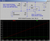
I have been trying different setups on my breadboard, and I am only able to utilize a range of circa 0.9v of the available 5v using a resistor.

Surely, as my adc accepts voltages from 0-5V, I should be able to make a circuit that allows my sensor to vary voltage from 0-5V so I may use full resolution.

How do I do this?

Thanks.M
 
Just setup a voltage divider with resistors and your sensor to create the largest possible voltage swing based on that 700 ohm change.
 
voltage divider to maximize voltage ratio (as mentioned above) - followed by opamp to maximize voltage swing from 0-5V

edit: an example is provided on attachment
 

Attachments

  • adc_conditioning.JPG
    adc_conditioning.JPG
    37.1 KB · Views: 303
  • plot.JPG
    plot.JPG
    10.6 KB · Views: 270
Last edited:
Hello,

Thank you for that. Yes, before I was only playing around with a voltage divider. It seems I get the biggest voltage ratio when resistance of r_bias is equal to the average of the highest and lowest resistance of r_var.

I am new to all this, and I have never played around with op amps. I was just out to buy one, and the resistors specified. Are you trying to subtract the sense voltage down, then scale it up? I have no idea how that circuit works, but the plot proves that I want to learn the concept. If you could I'd be very glad!

Kind regards,
Marius
 
Last edited:
The following is all based on ideal elements and such; but it's where you start.

Gain of Inverting OPAMP: (R2/R3)
Gain of Non-Inverting OPAMP: [(R2/R3) + 1]

If we feed the "sensed" voltage into the inverting side, and a reference into the non-inverting side; then we have something like this: (Vref * ((R2/R3)+1)) - (Vsense*(R2/R3)).

To balance everything out, we make R3 = R1.

Next we need to know is how to pick R2 and R3. Based on the voltage divider chosen to sample the "sensed" voltage, the maximum voltage swing is roughly 0.66V. We want to maximize this swing at the output of the OPAMP. If we want a 5V swing from a 0.66V swing, that comes out to roughly a 7.5 voltage gain. Picking 10k for R3 and R1 (nice number, not too stiff, not too soft); means that R2 would have to be 75k to provide the 7.5 voltage gain on the inverting input (where the "sensed" voltage is connected to).

Now for the reference voltage. With the configuration as shown, we want to set the reference to match the maximum voltage at the "sensed" input. That way when we do the "Vref-Vense" it will start at 0V (or close to). In our example, this turns out to be around 2.49V. R_ref1 and R_ref2 were made the same to split the 5V reference and picked at 1300 to match R_bias.

Hope this helps. National Semiconductor, Texas Instruments, and Analog Devices have loads of information on this.
https://www.electro-tech-online.com/custompdfs/2010/11/AN-31.pdf
https://www.analog.com/library/analogdialogue/archives/39-05/op_amp_applications_handbook.html
 
Last edited:
The following is all based on ideal elements and such; but it's where you start.

Gain of Inverting OPAMP: (R2/R3)
Gain of Non-Inverting OPAMP: [(R2/R3) + 1]

If we feed the "sensed" voltage into the inverting side, and a reference into the non-inverting side; then we have something like this: (Vref * ((R2/R3)+1)) - (Vsense*(R2/R3)).

To balance everything out, we make R3 = R1.

Next we need to know is how to pick R2 and R3. Based on the voltage divider chosen to sample the "sensed" voltage, the maximum voltage swing is roughly 0.66V. We want to maximize this swing at the output of the OPAMP. If we want a 5V swing from a 0.66V swing, that comes out to roughly a 7.5 voltage gain. Picking 10k for R3 and R1 (nice number, not too stiff, not too soft); means that R2 would have to be 75k to provide the 7.5 voltage gain on the inverting input (where the "sensed" voltage is connected to).

Now for the reference voltage. With the configuration as shown, we want to set the reference to match the maximum voltage at the "sensed" input. That way when we do the "Vref-Vense" it will start at 0V (or close to). In our example, this turns out to be around 2.49V. R_ref1 and R_ref2 were made the same to split the 5V reference and picked at 1300 to match R_bias.

Hope this helps. National Semiconductor, Texas Instruments, and Analog Devices have loads of information on this.
https://www.electro-tech-online.com/custompdfs/2010/11/AN-31-2.pdf
ADI - Analog Dialogue | Op Amp Applications Handbook

Thank you. That is fantastic!

Part 1:

I am at a very basic level, so I need teaching like a child. I need to understand the concept behind the design before I start to calculate values. I don't even feel comfortable with the op amp itself :D 
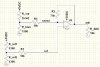
I am especially confused by the circuit that looks like loop going around the op amp. This is fantastically exciting, but a bit confusing.

Part 2:

I have made a test-circuit in my house. In the two voltage dividers, I use 1200ohm resistors + the sensor, because the actual resistance range of the sensor is precisely 962ohm to 1385ohm.

I use a 82k resistor instead of a 75k resistor (because, for some reason it seemed to give me voltage range that spans further down). Currently, my setup gives me a variable output of 0.92V when the sensor has a resistance of 962ohm, and 2.82V at 1385ohm. Which components needs altering to utilize more of the "voltage-band"? And more importantly: why?

Thanks!

Kind regards,
Marius
 
I am not sure I have all the time required to teach you how an OPAMP works (that's the reason I pointed you toward the two app notes). However, the resistor that loops back is called the feedback resistor and its main purpose is to convert the OPAMP from an open-loop system (where the gain is ideally infinite) to a closed-loop system (where the gain is tailored by you).

For the most part the app notes guide you to the basics of what type of circuit you are looking for (depending on what you're trying to do). From there is mostly math. After you come up with the topology and try out the circuit then you get some particulars which are specific to your problem and the device selection. I'll take a little better look at what you tried and suggest ideas (if you have a quick schematic, it makes it easier).
 
Last edited:
I totally understand that you don't have the required time to do that. And let's not forget how helpful you have been so far. Thank you Languer! :)

I will take a day off work tomorrow and try harder. I will post my progress. If you have the time to comment, I am sure I will find it very valuable! :)

Thanks :) M
 
Last edited:
Let's step through your problem again.

Using a span of 962-ohm and 1385-ohm, 5V supply and 1200-ohm as the other part of the voltage divider; we get the "sense" voltage can go from 2.78V to 2.32V (respectviely). That is a 0.450V voltage swing.

You're looking for a 5V swing: 5V_desired / 0.45V_actual = 11.01 => this says we want our gain around 11.

Remember that the "sense" voltage is feeding the inverting input. So we are looking for an inverting gain of 11, or R2/R3 = 11. Leaving R3 at 10k, means R2 should be set to 110k. Leave R1 same as R3 (10k).

Now the reference voltage is fed to the non-inverting input. The non-inverting gain is then, ((R2/R3)+1) = 12. If we were only feeding the the non-inverting input, the output voltage would reach 30.53V (now this is only in theory, because in practice the OPAMP would limit at or below the supply voltage - but this is how you do the analysis). This maximum voltage is what you want your reference to look like at the output of the OPAMP (remember this is only theoretical). At the inverting input, the reference voltage is desired to be at 2.54V (30.53/12). So you tweak you divider to give you around 2.54V.

Leaving R_ref2 at 1200, would set R_ref1 to around 1100.
 
Here is another way to do it. Use the same 5V supply as is used for the ADC reference to power it; that way, the circuit is ratiometric with respect to the ADC input range. You must use a modern CMOS Rail-to-Rail out OpAmp, like a TLC2272.

This method reduces the current through the thermistor to a few hundred uA, to minimize self-heating. This also linearizes the output from the OpAmp because the thermistor is driven from a "psuedo current source" instead of a voltage-divider. Tweaking just one resistor will center the transfer function in the ADC's range (if you are a little off on your resistor range.
 

Attachments

  • DF4.png
    DF4.png
    35.9 KB · Views: 288
Let's step through your problem again.

Using a span of 962-ohm and 1385-ohm, 5V supply and 1200-ohm as the other part of the voltage divider; we get the "sense" voltage can go from 2.78V to 2.32V (respectviely). That is a 0.450V voltage swing.

You're looking for a 5V swing: 5V_desired / 0.45V_actual = 11.01 => this says we want our gain around 11.

Remember that the "sense" voltage is feeding the inverting input. So we are looking for an inverting gain of 11, or R2/R3 = 11. Leaving R3 at 10k, means R2 should be set to 110k. Leave R1 same as R3 (10k).

Now the reference voltage is fed to the non-inverting input. The non-inverting gain is then, ((R2/R3)+1) = 12. If we were only feeding the the non-inverting input, the output voltage would reach 30.53V (now this is only in theory, because in practice the OPAMP would limit at or below the supply voltage - but this is how you do the analysis). This maximum voltage is what you want your reference to look like at the output of the OPAMP (remember this is only theoretical). At the inverting input, the reference voltage is desired to be at 2.54V (30.53/12). So you tweak you divider to give you around 2.54V.

Leaving R_ref2 at 1200, would set R_ref1 to around 1100.

Thank you. This was very helpful. Now I understand how the amplification works. Now my only remaining uncertainty is: is how can the 2.5 non-inverting input, combined with inverting input of 2.78V to 2.32 give an output of 0-5V? Maybe a simple formula would explain the relationship between the two.

Thank you! :) M
 
It's called superposition. You solve each side independently (just like the other side was not present - almost like that anyways), and then add the results.

Non-inverting Gain = 12
Vout of non-inverting side is (12*Vref)

Inverting Gain = 11
Vout of inverting side is (11*Vsense)

Vout is (12*Vref) - (11*Vsense)
 
Check the "Max Output Voltage" (when operated from single 5V supply) on the data sheet you referenced. Now go check it on the TLC2272 I referenced.
 
Last edited:
Check the "Max Output Voltage" (when operated from single 5V supply) on the data sheet you referenced. Now go check it on the TLC2272 I referenced.
You got it. The CA3140 is a replacement of the 741 which, even though legendary, is not to impressive. For what you're doing you require an OPAMP with an output which goes Rail-to-Rail (like the one MikeMl suggested - there are plenty others, that is just one good example).
 
Status
Not open for further replies.

Latest threads

New Articles From Microcontroller Tips

Back
Top