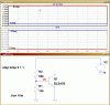
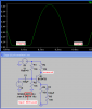
wait a minute , Feedback is a loop from output>feedback circuit>input>output , if we take emitter as output as you said , where is it connected to base ? i mean it is connected to base inside transistor, but where is the loop ??
Output is collector, input is emitter (as far as negative feedback is concerned).