Continue to Site

Welcome to our site!

Electro Tech is an online community (with over 170,000 members) who enjoy talking about and building electronic circuits, projects and gadgets. To participate you need to register. Registration is free. Click here to register now.

  • Welcome to our site! Electro Tech is an online community (with over 170,000 members) who enjoy talking about and building electronic circuits, projects and gadgets. To participate you need to register. Registration is free. Click here to register now.

Gain control in Amplifier

Status
Not open for further replies.

neptune

Member
hello,
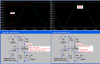
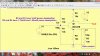
can any body explain to me how gain control works, i have marked the gain control and posted the circuit for you to see.
when i remove this series RC network called gain control i get zero DC output.
what is happening here ?
 

Attachments

  • amplifier.asc
    1.5 KB · Views: 139
  • amp.jpg
    amp.jpg
    451.4 KB · Views: 243
that's not really a "gain control" as much as it is an emitter resistor bypass. it's purpose is to maintain high gain above the cutoff frequency set by the combination of the RC network, and low gain at DC (actually NO gain at DC because of the input capacitor). the corner frequency of this RC network is about 16hz. when you remove the RC network, the AC gain is reduced to about 1 (i.e. the circuit becomes a unity gain inverter)
 
Last edited:
The reason for the emitter resistor is to help maintain a stable DC bias point for the transistor. Since this reduces the gain, a bypass circuit is used to increase the gain for the desired AC frequencies.
 
it's purpose is to maintain high gain above the cutoff frequency set by the combination of the RC network,
which RC network are you talking about ? is there a cutoff frequency in amplifier ?
 
The reason for the emitter resistor is to help maintain a stable DC bias point for the transistor. Since this reduces the gain,
it doesnt reduces gain it makes it 0 gain
 
it doesnt reduces gain it makes it 0 gain
Well, 0 is certainly reduced gain.;)

But the problem with the circuit is that the DC bias point operates the transistor near the saturation region (look at the collector and emitter voltages). You need to bias the transistor in the active region (reduce the base voltage) to achieve proper amplification.
 
Last edited:
tnx cs... just got home from work and was going to figure out the math on this one, but you beat me to it. i figured the base bias must have been a bit high if he was getting close to nothing on the output, and that voltage divider looked a bit strange, except the emitter resistor was also 10k, which would provide local degeneration to the point where the transistor might be inside the linear range. if there's 4.5V on the base, the emitter voltage will be about 3.8V, so the emitter current is 380uA, the collector current is 378uA, and the base current is 2uA (380ua/178(the beta of the transistor model)). since the collector current is 380uA, the collector voltage is at 9-3.78=5.22V. this approximates the results of the sim itself which came up with 2.16uA base current, 380uA collector current, and 382uA emitter current. there's about 1.4V between collector and emitter. the transistor isn't in saturation, but it's not far from it.
 
But the problem with the circuit is that the DC bias point operates the transistor near the saturation region (look at the collector and emitter voltages). You need to bias the transistor in the active region (reduce the base voltage) to achieve proper amplification.
i just want to know why we need to pass AC signal (in R5 and C1) seperately from emitter resistance (R4) , when they both go to ground invariably.
I know without R5 and C1 in series there is no gain in transistor , but what am i missing here ?
 
i just want to know why we need to pass AC signal (in R5 and C1) seperately from emitter resistance (R4) , when they both go to ground invariably.
I know without R5 and C1 in series there is no gain in transistor , but what am i missing here ?

R5 and C1 reduce the AC negative feedback in the stage, giving it gain - without it the AC gain is set by the ratio of the emitter and collector resistors (R5 is placed in parallel with the emitter resistor - for AC only - altering that ratio).

For maximum gain (no negative feedback) R5 should be a piece of wire.
 
i just want to know why we need to pass AC signal (in R5 and C1) seperately from emitter resistance (R4) , when they both go to ground invariably.
I know without R5 and C1 in series there is no gain in transistor , but what am i missing here ?

hi,
The stage gain of a single Class A transistor amplifier with an Emitter resistor is approx Collector resistor/Emitter resistor.

When the Emitter resistor is bypassed by a capacitor, the cap has a reactive impedance that decreases with frequency.
This Xc impedance is in parallel with the fixed Emitter resistor.

As the frequency of the AC signal increases the impedance of the cap reduces,,,, so the stage gain becomes G= Rcollector/[Parallel value of the fixed resistor and Xc],,, the stage Gain increases.

If the AC signal was say 1KHz and the bypass cap 10uF, the Xc would be 16R.!!
 
Last edited:
tnx cs... just got home from work and was going to figure out the math on this one, but you beat me to it. i figured the base bias must have been a bit high if he was getting close to nothing on the output, and that voltage divider looked a bit strange, except the emitter resistor was also 10k, which would provide local degeneration to the point where the transistor might be inside the linear range. if there's 4.5V on the base, the emitter voltage will be about 3.8V, so the emitter current is 380uA, the collector current is 378uA, and the base current is 2uA (380ua/178(the beta of the transistor model)). since the collector current is 380uA, the collector voltage is at 9-3.78=5.22V. this approximates the results of the sim itself which came up with 2.16uA base current, 380uA collector current, and 382uA emitter current. there's about 1.4V between collector and emitter. the transistor isn't in saturation, but it's not far from it.
Hello can you tell me step by step guide online to plot transistor characterstics graph
 
Hello,
The stage gain of a single Class A transistor amplifier with an Emitter resistor is approx Collector resistor/Emitter resistor.
then what is Beta = I(collector)/I(base) ?

As i see through Simulation, 240uA AC is flowing through R5 and C1, and meagre 4uA AC is flowing through R4 ,Only 4uA AC Reaches R1. so there is a very little negative feed back to input which is 180 degree out of phase with out put signal.
so instead of seperating DC and AC signals at emitter we should take very high value of emitter resistance to give feedback.

I experimented this and cutted out R5 and C1 from emitter , Vout decreased but not much.
 
I experimented this and cutted out R5 and C1 from emitter , Vout decreased but not much.
Didn't you use the simulation that you posted?
With C1 and R5 the signal output is 1.15V peak. The voltage gain is 1.15V/0.02V= 57.5.
With C1 and R5 removed the signal output is 0.02V peak which is the same as the input level. The voltage gain is 1.

Maybe you measured the DC output.
 
hello Audio,
I experimented this and cutted out R5 and C1 from emitter , Vout decreased but not much.
my bad ! there was some simulation mistake.

Can you explain to me the current flow in C1+R5 and R4, and how do they give negative feedback to base of transistor via R1 resistance when they themselves are grounded ?
 
any voltage applied to the emitter in phase with the signal on the base is called negative feedback (a more accurate term is degenerative feedback, since it's effectively in series with the transistor itself, not following a separate path). with a short from the emitter to ground, there is no local feedback. with a resistance, a voltage is developed from the emitter current, reducing the amount of base current.
 
The voltage gain of the transistor (with no load) is the collector resistor divided by the emitter resistor in series with the small internal emitter resistance of the transistor. Without C1 and R5 the voltage gain is a little less than 10k/10k= 1.

Capacitor C1 is a dead short circuit at audio frequencies. Then the simply calculated voltage gain is a little less than 10k/10k parallel with 100 ohms= 101. The internal emitter resistance is about 74 ohms at this low DC current so the actual voltage gain is 10k/(100 + 74)= 57.5.

You do not need to think about currents and negative feedback, the transistor circuit does that. The currents in R4 and R5 apply negative feedback to the emitter not to the base at R1.
 
The voltage gain of the transistor (with no load) is the collector resistor divided by the emitter resistor in series with the small internal emitter resistance of the transistor. Without C1 and R5 the voltage gain is a little less than 10k/10k= 1.
Q> If Voltage gain Rc/Re then can we simply reduce emitter resistance to increase the gain ?
Q> so when we connect some load at output then do we need these gain control i.e. C1 and R5 are not needed. ?
Capacitor C1 is a dead short circuit at audio frequencies. Then the simply calculated voltage gain is a little less than 10k/10k parallel with 100 ohms= 101. The internal emitter resistance is about 74 ohms at this low DC current so the actual voltage gain is 10k/(100 + 74)= 57.5.
Actually if we calculate Xc of capacitor at that given frequency(200Hz) it is 78.5ohm and tottal Impedance of that RC arm is Z= 127ohm so why do you consider capacitor dead short ?
You do not need to think about currents and negative feedback, the transistor circuit does that. The currents in R4 and R5 apply negative feedback to the emitter not to the base at R1.
Can you elaborate a little theory here.
A feedback is said to be from output to input of any circuit , Where do the feedback start from and where do it end in this circuit ?
 
Hi,

The two main goals of a circuit like this are to achieve some required level of AC gain while at the same time keeping the DC bias point as constant as possible with temperature. With low values of emitter resistance both the AC gain and the DC gain are high, but the DC bias point varies considerably. With somewhat higher values the DC bias point becomes more and more stable with temperature but we start to loose too much AC gain.
Choosing a value of emitter resistance that provides some AC gain and allow for some decent temperature stability means getting a lower than required AC gain but keeps the temperature stability within an acceptable range. Because we lost some AC gain in obtaining better temperature stability, we look for a way to increase the AC gain while not affecting the DC gain too much.
We know from experience that a capacitor passes AC current but mostly blocks DC current. By adding a bypass cap (or network) across the emitter resistor we get a higher Rc/Xe ratio for AC but maintain the same Rc/Re ratio for DC. This allows us to increase the AC gain while not affecting the DC gain too much and thus get more of the required AC gain while maintaining the desired temperature stability. (Note Xe here is an approximation of the emitter resistance in parallel with the emitter bypass capacitor reactance).

The degenerative feedback starts when the input drive increases which would cause the output current to increase. We get this because the base voltage has to rise up a little and we'll call this increase Vx. Now a change of Vx for a given amplifier would normally cause an output change of Ix amps, which is about the same as the emitter current. The emitter current passes through the emitter resistor, and that develops a voltage increase. So we have the input voltage increasing that caused a higher output current which in turn caused a higher emitter voltage. But the increase Vx could only cause an increase in output current because that voltage appears across the base emitter junction. If that voltage was reduced, there would be less output current. Well, when the current increases and causes the emitter voltage to rise that means that we have a higher emitter voltage as well as base voltage so the overall effect is to reduce the effective input voltage and thus it reduces the gain.
For a quick numerical example, say we have 2.7v on the base and 2v at the emitter. Now we increase the input signal which in turn causes an increase in base voltage of 0.1v, which brings it up to 2.8v. Naturally the output current is going to increase because now the base emitter voltage is 0.8v. The higher current flowing through the emitter causes a higher voltage drop across the emitter resistor, say an increase of 0.05v. Now when we look at the base emitter voltage it has reduced to 0.75v. It's still higher than it was before we increased the input voltage (it was only 0.7v before) but it's less than the total caused by the input signal increase itself, which would have been 0.8v. Thus, the current flowing through the collector (and thus emitter) caused the input signal to look like it was less than it really was, and thus the output goes not go up as high as it would have without that emitter 'feedback' mechanism.
If this still isnt clear, then do a DC simulation of this amplifier and look at the emitter voltage and the voltage across the base emitter junction. Note the emitter voltage and create a voltage source that will hold that voltage constant (battery). Then increase the input voltage DC component by a small amount. Note the change in collector current and the voltage across the base emitter. Next, remove the battery and repeat using the same input voltage increase. Note the output current again and also the base emitter voltage again. You should see less change than before and the emitter voltage will have risen a little higher.
(Note to increase the input DC component in a static simulation, insert a small battery in series with the base, like say 0.1v, but you may have to go lower like 0.05v or 0.01v to get reasonable results).

Most practical amplifiers have a collector resistor value that is higher than the emitter resistor unless they are for some special purpose.
 
Last edited:
Q> If Voltage gain Rc/Re then can we simply reduce emitter resistance to increase the gain ?
Yes, I simulated it and got a max voltage gain of 182.5 when R5 is shorted and there is no load. But with maximum gain then the distortion is extremely high when the output level is fairly high. R5 adds negative feedback which reduces the voltage gain and reduces the distortion.

Q> so when we connect some load at output then do we need these gain control i.e. C1 and R5 are not needed. ?
An output load is parallel with Rc so it reduces the voltage gain. You might need C1 and R5 to further reduce the voltage gain and reduce distortion.

Actually if we calculate Xc of capacitor at that given frequency(200Hz) it is 78.5ohm and tottal Impedance of that RC arm is Z= 127ohm so why do you consider capacitor dead short ?
A telephone circuit might cut bass frequencies below 200Hz. In your circuit, C1 is 100uF and R5 is 100 ohms so their cutoff frequency is at 16Hz where they reduce the maximum gain by 3dB which is 0.707 times. At 1kHz the reactance of the 100uf capacitor is only 1.6 ohms (almost a dead short) and is lower at higher frequencies.

A feedback is said to be from output to input of any circuit , Where do the feedback start from and where do it end in this circuit ?
The negative feedback created by an unbypassed emitter resistor cancels some of the input signal between the base and the emitter. The emitter is not the output in your circuit but it could be an output.

Here is a simulation of a transistor circuit with a low input signal level then a higher input signal level when the voltage gain is maximum because the emitter resistor is bypassed by a capacitor:
 

Attachments

  • transistor simulation.PNG
    transistor simulation.PNG
    42.4 KB · Views: 176
Last edited:
The negative feedback created by an unbypassed emitter resistor cancels some of the input signal between the base and the emitter. The emitter is not the output in your circuit but it could be an output.
wait a minute , Feedback is a loop from output>feedback circuit>input>output , if we take emitter as output as you said , where is it connected to base ? i mean it is connected to base inside transistor, but where is the loop ??

Everything is going to ground that is what is confusing from start :(
 
Status
Not open for further replies.

New Articles From Microcontroller Tips

Back
Top