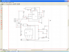
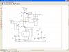
Move C1 left next to the LM358
Why the long trace that connects R3 with the LM358 flip it horizontal and attach to the trace that is right next to it
or
Take the trace going around R4/R6 underneath R4/R6, then no need for the link wire
Modified the image with second option since it was easier, first option still preferred
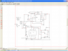
There is a lot of wasted space on the board
Capacitor polarity is all over the place same with the diodes, going to make it a pain to stuff the board if you don't have a silkscreen.
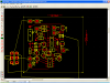
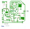
View attachment 31030