Continue to Site

Welcome to our site!

Electro Tech is an online community (with over 170,000 members) who enjoy talking about and building electronic circuits, projects and gadgets. To participate you need to register. Registration is free. Click here to register now.

  • Welcome to our site! Electro Tech is an online community (with over 170,000 members) who enjoy talking about and building electronic circuits, projects and gadgets. To participate you need to register. Registration is free. Click here to register now.

Failed EMC with 60W offline Flyback LED driver

Status
Not open for further replies.

Flyback

Well-Known Member
Hello,
We recently took our 60W Offine , isolated, PFC’d Flyback LED driver (schematic attached) for Conducted and Radiated EMC scans.
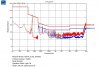
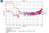
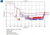
The conducted EMC scan fails at a few spot frequencies as the attached shows.
We also failed Domestic Radiated emissions (CISPR F). –But we passed on Industrial Radiated emissions (CISPR B).

The problem is, that we have no more room on the PCB for any more filter components. As it was, we had to use SMD Y2 capacitors on the bottom of the board because there is no room on the PCB for radial ones.
I believe we need a second common mode choke, but there is no room on the board.
Are there any tricks we can pull off here?...unfortunately we aren’t allowed to make the board any bigger.

The ceramic Y2 caps were 3.3nF….but as you know, ceramic X7R capacitors are unfortunately only around 10% of nominal value when operated at rated voltage.

The 60W Flyback’s FET and Diode had small TO220 heatsinks directly connected to them..The FET heatsink is then obviously connected to the drain tab of the FET.…..however, do you agree that this would have made the Radiated scan result worse? (…I believe we should have had an insulating pad between FET heatsink and the FET itself, do you agree?)

During the scans, we had a 60W LED load that we “hacked” together connected……Unfortunately, due to the “hacked nature”, much of the wiring in the LED load bank was not twisted and so there were wide area current loops. The LEDs were on bits of MCPCB, and these were not connected to Earth. The secondary 0V was just “floating”.


(We passed Mains Harmonic Emissions and Power Factor)
------------------------------------------------------------------------------------------------------------------
Some of the datasheets of our filter components…………
VJ2220 SMD X2 and Y2 capacitors
https://www.vishay.com/docs/45020/vjsafetycapsx7r.pdf

ELC09D inductors
www.farnell.com/datasheets/2245397.pdf

Wurth 7448640415 Common Mode Choke
https://katalog.we-online.com/pbs/datasheet/7448640415.pdf
 

Attachments

  • Conducted EMC scan.jpg
    Conducted EMC scan.jpg
    84.1 KB · Views: 161
  • Mains Input Filter _60W Flyback _1.pdf
    22.6 KB · Views: 144
Last edited:
Your schematic has both filter caps connected between live and earth, rather than one each live-earth and neutral-earth.
If the board is actually built like that, it could be the problem. The neutral connection has least suppression overall.

Also, what are the rectifier diodes? Some types can cause high frequency spikes & in RF gear it's not unusual to add a small cap across each diode to limit that. Alternately, use fast recovery types rather than extra components, to fit your board limit.
 
Your schematic has both filter caps connected between live and earth, rather than one each live-earth and neutral-earth.
Youre right, totally missed that.
As for the diodes, I would rather use soft-recovery ones if possible.
Another thing that I don´t like is the primary-secondary Y cap connected between the high side and the output ground, I would rather see it connected ground to ground.

Some snubbing around Q1 could help also if it is not there.

All in all, conducted common mode emissions are usually mainly caused by parasitic capacitance to case and subsequently PE. Does Q1 have any heatsink? Where is it electrically connected? Same case with the aux supply.
If possible and if it is conductive, try electrically bonding the core of the transfomer to primary gnd.
The Y2 caps maybe could have a little larger value? I think the standard allows up to 4n7 at 230V (1mA earth current IIRC?)

While you were there, you should have tried disconnecting each power supply to see what to focus on.
Next time I would prepare a bunch of different mods and see what helps and what doesn´t.
 
woops (concerning Y caps) ...sorry!!!...now corrected in above post....(it wasnt like that in the circuit)
 
Last edited:
Does Q1 have any heatsink? Where is it electrically connected? Same case with the aux supply.

Q1 has a heatsink which is screwed directly to the drain tab of the TO220 FET. (no thermal pad between)

The TNY287 Flyback controller is an SO8 package, and the source of the internal FET (a quiet node as you know in a flyback) is brought out to pins 1-4 for connection to thermal copper pour on PCB

If possible and if it is conductive, try electrically bonding the core of the transfomer to primary gnd.

Thanks, presumably this is to induce the switching node inside the transformer to couple to the core instead of coupling away to earth outside the enclosure,? hence preventing a common mode noise issue?
 
Thanks, ...In the meantime, we did another quick Conducted EMC scan, this time with the attached EMC filter. This performed much worse than the first EMC filter (shown in the top post). This worse conducted EMC scan (on 8th November) is also shown attached here. (the better scan of 22nd August is also attached here, for ease of reference)

We believe that the worsening is due to the fact that we no longer have a Y capacitor from primary to secondary of the 500mW bias supply transformer. We also believe that the change to using Radial Y capacitors in the AC part of the filter, as opposed to SMD ones as used in the previous scan, has also had an impact. –This being due to the increased stray inductance of the radial Y capacitors.
Also, in the worse scan, our LED load was sitting on a much bigger heatsink. Also, in the worse scan, the Power NFET was screwed to a bigger metal heatsink. (the tab of the FET being the switching node means that this made EMC worse).

So do you agree that we need to have Y capacitors between primary and secondary of both transformers in order to improve things?

I have also attached the (better) previous scan of 22nd August here. (Also the EMC filter schematic is also atttached)
 

Attachments

  • EMC filter _22nd August.pdf
    23 KB · Views: 145
  • Conducted EMC scan _22nd August.jpg
    Conducted EMC scan _22nd August.jpg
    84.6 KB · Views: 160
  • EMC filter _8th November.pdf
    25 KB · Views: 135
  • Conducted EMC scan _8th November.jpg
    Conducted EMC scan _8th November.jpg
    86.9 KB · Views: 141
Last edited:
From my experience it is really worthwile to buy or build your own lisn, so that you can do your almost real pretest and tweak the componets.
 
Last edited:
Thanks, we identified a Rigol Spec Anal. and a Hameg HM6050 LISN, but we dont know if the Rigol spec anal. comes with transient protection of its signal input.?...If it doesnt then a transient on the mains can blow it up, and it costs thousands.

This was our costing of personal EMC kit.....The total is £4022, and then you have to pay £800 a year for calibration.

DSA815 spectrum analyser = £1300
Including the following necessary options for DSA815 spec analyser..
-Advanced Measurment kit (AMK-DSA800) = £423
-VSWR-DSA800 = £400
-EMI-DSA800 = £454
S1210 EMI pre-compliance software = £450

HAMEG HM6050 LISN = £1000

DSA815 spectrum analyser for Conducted EMC measurement…
https://www.rigolna.com/products/spe...lyzers/dsa800/

HM6050 LISN:
https://uk.farnell.com/rohde-schwarz/...ion/dp/2057576
 
you might also want to try replacing the rectifiers with silicon carbide rectifiers. normal and shottky silicon rectifiers have a reverse recovery characteristic that allows a reverse current spike when driven into the reverse region. try silicon carbide (SiC) rectifiers in place of the silicon. SiC doesn't have reverse recovery, so SiC rectifiers should be "quieter". if you can work around the difference in forward voltage for SiC (2V rather than 0.7V), it should help.
EDIT:
well... that was interesting... when SiC rectifiers first came out, the big advantage was "zero reverse recovery time"... apparently they do have reverse recovery, but it's very short compared to other diode technology. in any case, SiC would be a good choice for reducing RF noise. more info available here: https://www.rohm.com/documents/11303/2861707/sic_app-note.pdf
 
Last edited:
Thanks, you are right, in fact, on the main 60W flyback, we operate in DCM, so we dont get reverse recovery, but the small flyback, it switches kind of randomly and i think sometimes in CCM...so we will look at SiC for the small flyback output diode, thanks.
 
Status
Not open for further replies.

Latest threads

New Articles From Microcontroller Tips

Back
Top