Continue to Site

Welcome to our site!

Electro Tech is an online community (with over 170,000 members) who enjoy talking about and building electronic circuits, projects and gadgets. To participate you need to register. Registration is free. Click here to register now.

  • Welcome to our site! Electro Tech is an online community (with over 170,000 members) who enjoy talking about and building electronic circuits, projects and gadgets. To participate you need to register. Registration is free. Click here to register now.

Env Monitor circuit, WAS: (... optional processing stages)

Status
Not open for further replies.

Gandledorf

New Member
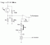
Say I have some signal of interest on voltage, and I am processing it using several stages. For instance, I have a gain stage, bandpass stage, ADC stage, and then a demodulation stage.

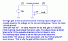
If I wanted to include several options for one of the stages, say in one trial I want to bandpass with one filter, and in another trial, with a different filter, or perhaps I want the option to remove a stage, possibly strip away the gain stage to see if I can get good results with the built in gain of my filter, can I do this in the following manner?

**broken link removed**

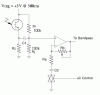
Would the 2N3904 be an appropriate transistor as it has a fairly low current gain? How would I need to account for this gain in my circuit?
 
Bipolars don't work very well in this application. There are analog multiplexer chips made for this purpose. Look at CD4066 and 74HC4066 or 74HCT4066.
 
If I understand your schematic, the only useful functions you can perform with your multiplexer are gain in, gain out, and no signal. If you don't need "no signal", consider the attached. The reason I suggest this scheme is that you are going to need an op amp as a buffer to the input of your filter anyway, because its input resistance is Rg, which is probably too much load for the optical receiver. The circuit below allows the operational buffer to be switched between unity gain and whatever you choose with the pot.
If you want other functions from your MUX, what are they?

Oh - I added a resistor to ground from your phototransistor emitter. I don't think it will work without it.
 

Attachments

  • secchi.gif
    secchi.gif
    16.2 KB · Views: 942
Thanks again for the help Ron, that was really what I was trying to do, either remove or include the amplifier stage.

I have some questions though, about your diagram, as I don't understand it completely. I've attached a shortened version of it, with labels for reference. Tell me if I have any of this right...

The op-amp, Ra1, Ra2, and Rb form a non-inverting amplifier, with a gain of 1 + RB/(Ra1 + Ra2). C2 appears to be a decoupling capacitor? I'm not sure on this one, nor am I sure why triggering the MUX, and thus pulling one side of the capacitor to ground will turn off the amplifier.

Ri, and Rj appear to be forming a voltage divider of value 1/2, though the includsion of the transistor signal along the center is confusing to me, as is the capacitor C1. Is Rz just serving as a current load for the transistor? I'm very confused here.
 

Attachments

  • secchi2.gif
    secchi2.gif
    5.1 KB · Views: 756
You have every reason to be confused. I screwed up. Below is a modified schematic. The gain is, as you know, 1+Rb/Ra, so if Ra=infinity (switch off), Gain=1, which still gives you the buffering (low output impedance) you need to drive the filter.
Rz is as you described. The phototransistor passes current proportional to illumination. It needs a load to develop a voltage. C1, Ri and Rj assure that the input voltage to the op amp stays centered between the rails, giving you maximum dynamic range. C2 keeps the DC gain at 1, so the output voltage is also centered between the rails. Consider what would happen if C2 were shorted. (Solution left to the student. :) )
 

Attachments

  • secchi2_117.gif
    secchi2_117.gif
    5.3 KB · Views: 688
If C2 were shorted b/w V+ and GND, it would act to store charge for the circuit, correct, I don't see how this would be "bad" per say.

I still don't understand the operation of the coupling capacitor (c1), and Ri, Rj. Or why C2 keeps the DC gain at 1.

Does C1 act to block DC? I'm really unclear how Ri and Rj are interacting with the input line. Were it just a voltage divider, I'd understand it, but as is, it's a little unclear, especially with the capacitor in there.
 
Gandledorf said:
I still don't understand the operation of the coupling capacitor (c1), and Ri, Rj. Or why C2 keeps the DC gain at 1.

C2 keeps the gain at 1 because you have 100% DC negative feedback through the pot, C2 reduces the AC feedback as it brings the extra resistor it has in series with it in circuit for AC. The exact same system is used in audio amplifiers, and for exactly the same reasons.

Does C1 act to block DC? I'm really unclear how Ri and Rj are interacting with the input line. Were it just a voltage divider, I'd understand it, but as is, it's a little unclear, especially with the capacitor in there.

C1 provides DC blocking, you only want the AC signal content from the photo-transistor - otherwise the variations in ambient light would upset the opamp biasing. Ri and Rj simply provide DC bias for the opamp, presumably it doesn't have a split supply?.
 
Does the DC blocking for C1 matter all that much considering we're about to bandpass the signal? I would think the DC would get sorted out there, is this not so? How would one pick an appropriate value for C1, and Rz?

You are correct, I don't have a split supply, it's simply +5V, and GND, from a battery with a 7805.

Could you give me any more details on how Ri and Rj interact with the signal? I'm having difficulty working it out.

Presumably, our transistor gates b/w 0 and 5V, based on the amount of light it picks up. If we just look at Ri and Rj alone, they act as a voltage divider, setting up the potential at that point for 2.5V. It seems like in some cases, this would cause there to be no signal sent through to the op-amp? I'm just very confused as to the reasoning behind this. Perhaps there is a reference on this topic somewhere which I could consult?
 
Gandledorf said:
Does the DC blocking for C1 matter all that much considering we're about to bandpass the signal? I would think the DC would get sorted out there, is this not so? How would one pick an appropriate value for C1, and Rz?

Yes, the DC blocking is very important, otherwise the DC conditions of the opamp will vary with the ambient light levels. You pick C1 to have a suitably low impedance at your modulation frequency, Rz would be chosen to provide a suitable range of operation - based on how it will be affected by ambient light levels - so select it for around 2.5V at a mid level of light.

Could you give me any more details on how Ri and Rj interact with the signal? I'm having difficulty working it out.

Ri and Rj don't interact with the signal at all, they are simply used to generate a mid HT point, essentially a simple split supply.

Presumably, our transistor gates b/w 0 and 5V, based on the amount of light it picks up. If we just look at Ri and Rj alone, they act as a voltage divider, setting up the potential at that point for 2.5V. It seems like in some cases, this would cause there to be no signal sent through to the op-amp? I'm just very confused as to the reasoning behind this. Perhaps there is a reference on this topic somewhere which I could consult?

No, the transistor current will vary with the ambient light, and have a small (perhaps VERY! small) amount of modulated signal on it. The capacitor blocks most of the large variations from the ambient light, allowing the required modulation to be amplified. The voltage on the potential divider has nothing to do with the signal, it simply biases the opamp, and sets the input impedance (at Ri and Rj in parallel).
 
Ok, I think I almost have it. Is the diagram below represenative of the effect?

The first signal is that sent out by the emitter, the second, is that seen by the transistor (very roughly). The DC blocking capacitor eliminates a lot of the mess, and makes it closer to the original diagram.

The third diagram is after the biasing resisitors. I assume this has something to do with the "virtual ground" I remember hearing about in lab? So the biasing resistors create a virtual ground at 2.5V, allowing the signal to be amplfied around that virtual ground?
 

Attachments

  • signal_159.gif
    signal_159.gif
    5.6 KB · Views: 637
I think you're getting it. Hopefully your "DC noise" won't have such fast edges.
"Virtual ground" doesn't apply to the biasing scheme. It's just a voltage divider with an AC signal coupled onto it. I have attempted to explain the concept of virtual ground below. You might find a better explanation with a Google search.
I would make Rb a 100k pot. Letting Ra=10k will give you a gain range of 1 to 11. If you do this, pick C2 in the range 3.3nF to 4.7nF. Let C1~560pF to 1000pF. Both of these caps form highpass filters, and I have chosen values that make the -3dB corner frequency~5kHz, so that they pass your carrier with little or no effect on the gain, and still get rid of a lot of low frequency crap.

F3db=1/(2*pi*R*C)

For C1, R is the parallel resistance of Ri and Rj. The impedance of your receiver actually needs to be added in to be accurate, but the exact cutoff frequency isn't critical, and we don't have a value for Rz yet.
For C2, R=Ra.
 

Attachments

  • opamp.GIF
    opamp.GIF
    10 KB · Views: 613
Am I at least correct in the assumption that, where the signal (without noise) goes from 0 to X volts, after the biasing, it goes from 2.5-X/2 volts to 2.5 + X/2 volts?
 
Gandledorf said:
Am I at least correct in the assumption that, where the signal (without noise) goes from 0 to X volts, after the biasing, it goes from 2.5-X/2 volts to 2.5 + X/2 volts?

Although I've just got back from the pub, and am not 100%, that sounds about right :p

However, it's not something you should be bothering about at all - you are trying to amplify the modulation on the IR signal - this is totally separate to any DC conditions on the opamp. So the small AC signal from the phototransistor is fed through the capacitor and amplified by the AC gain of the opamp. The AC gain is set by the feedback resistor (which is shown as a pot) and the resistor in series with the capacitor (standard non-inverting opamp gain formula).
 
Nigel Goodwin said:
Gandledorf said:
Am I at least correct in the assumption that, where the signal (without noise) goes from 0 to X volts, after the biasing, it goes from 2.5-X/2 volts to 2.5 + X/2 volts?

Although I've just got back from the pub, and am not 100%, that sounds about right :p

However, it's not something you should be bothering about at all - you are trying to amplify the modulation on the IR signal - this is totally separate to any DC conditions on the opamp. So the small AC signal from the phototransistor is fed through the capacitor and amplified by the AC gain of the opamp. The AC gain is set by the feedback resistor (which is shown as a pot) and the resistor in series with the capacitor (standard non-inverting opamp gain formula).
What he said - keeping in mind that I just had a glass of wine. :)
 
Status
Not open for further replies.

Latest threads

New Articles From Microcontroller Tips

Back
Top