Electro Tech is an online community (with over 170,000 members) who enjoy talking about and building electronic circuits, projects and gadgets. To participate you need to register. Registration is free. Click here to register now.
Welcome to our site! Electro Tech is an online community (with over 170,000 members) who enjoy talking about and building electronic circuits, projects and gadgets. To participate you need to register. Registration is free. Click here to register now.
Pads can not be used as vias. If the board is double sided and pads are plated they can be considered to be vias as well. They are normally part of a component.
However if you plan to design a single sided board with wire jumps instead of a double sided board with vias, generated by Eagle when switching layers from e.g. bottom layer to top layer while routing you can use pads which will remain pads (component). Placing two pads (preferably along a straight line) they are treated like components, meaning they have to be connected somewhere.
Note that the "vias" have a point of origin (white cross in the center), hence they are components. Vias have no origin.
- How can i Keep eagle from turning component Pads in to vias?
I'm even more baffled now but I will try to explain more:
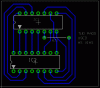
I would like to create a PCB with a mix of smd and TH components
I would like to have the TH components only have a pad on 1 side.
The reason for this is that if I will do some rework on it the
components are too hard to desolder on DS pads.
I noticed that eagle (autorouter) is using some of the pads as via's
(I can see that from the color of the traces that go to the pads)
but I prefer not to have that.
The pad of a TH component by definition exists on both sides of the PCB. A SMD pad exists only on one layer.
Even if you could get a pad on one layer the PCB plating process would plate the hole and it would be even harder to desolder. You do not want this.
You can easily remove through hole parts by cutting the leads off the component. Then desolder the leads one at a time.
Rather then remove solder I add a bit more and give the board a sharp rap on the bench such that the liquid solder and the bit of lead leave the hole at high speed. Do not break the board. Others use solder braid or solder suckers.
Few people use the auto router. If you want the job done right route the traces by hand.
Using SMD and through hole parts for a PCB design you should "mirror" your SMD parts to appear on the solder side. That way you can route traces without using wire jumps or the top layer, provided you find a way to connect them.
If there is no other way than using the top layer to route you might "change layer" and route on top.
Caution: Even if you have planned to use wire jumps you should inform your PCB manufacturer to make the board single sided! PCB manufacturers go by the board design when making the board and if there are traces on the bottom and top layer the result will be a double sided board with plated through holes respectively plated vias.
Post your schematic here and I'll take a close look at it.
This site uses cookies to help personalise content, tailor your experience and to keep you logged in if you register.
By continuing to use this site, you are consenting to our use of cookies.

")