Jeremy is using water cooling at about 20C. I can't find where he did the measurements but as I recall he only had a case temperature rise of about 4C on the last FET in line so it is almost an infinite heat sink. He also measured the top of the TO220 and got a number very close to the calculated junction temperature so I almost belive it.
I don't want to dispute anyone's work, but I can't really explain that other than if some kind of mistake was made somewhere along the way. I don't recall the exact specifics, but when I was doing my preliminary testing with ~6 transistors and ~100 Watts on virtually the same heat sinking apparatus, I was getting a higher indicated Watts to temp ratio. The backs of the FETS were getting pretty hot too. My best guess would be that he is likely not putting all the Watts into the device that he thinks he is.
If that's not it, and there are no other errors, then this data alone would make it seem perfectly sound to go ahead with four, three, or even two transistors at 2000 Watts. And that just seems completely unrealistic to me. Even with resoundingly positive data, I can not recommend going forward with something like that. It goes against what I would consider transistor common sense.
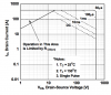
() The big difference in this FET is the thermal resistance junction to case for this guy is only 0.05C per watt whereas a TO3 like the 3055 has a junction to case of 1.5C/watt. So it is 30 times better getting the heat from the die to the case.
Yeah, if we are just talking whats better or worse when compared to the other parts, then I'm with you guys. Those are better performers on paper. I just want to make sure we are not using the numbers to assume we can get 2~4 transistors to dump 2000 Watts of heat. Doing that will almost certainly destroy them no matter what the heat sinking is, I'm fairly sure of it.
I'm not sure how they do that...
I'm thinking larger die most likely. Spreading the heated area out will lower the effective thermal resistance. It costs much more to make the larger die though. If it isn't that, then they are putting a thermal bridge on the top and sides of the die that transferred heat around to the tab. This would have the effect of more surface area without increasing the die area. I don't even know if they do that or not though, but it seems reasonable to accomplish. The only other thing they could possibly be doing would be to not use silicon. They would have to be using something else with a higher thermal conductivity. Crystalline silicon is already fairly high thermal conductor though, so to be a material with even better thermal performance it would have to be some crazy exotic semiconductor made with like diamond, carbon nano tubes, or silver-oxide or something. Even so, if they were doing that, then the limiting factor would just get shifted over to the copper tab.
Maybe we should de-encapsulate some power transistors some time, and see what is really going on. I'm fairly sure they will not look much different from the images I posted though.
Final thoughts
I hate to drag things out for a long time, and I hate to be a naysayer on something I helped come up with. However, I would hate to have this be dangerous and unreliable even more so. As far as I am concerned, using the package as an indicator of wattage is the only guarantied reliable method for choosing the transistor, as it is a manufacturer independent metric. Anything else is dubious and would need to be thoroughly field tested before it could be deemed reliable. Using the datasheet numbers on something like this depends solely on the manufacturer both knowing what they are doing, and them not pushing marketing into the equation. Both of these things are far from a guarantee, even with a good manufacturer.
 With 2 or 3 of those babies we wouldn't need to worry about lowering the current at 50 volts (just the house circuit breaker). $13 isn't cheap, but it would sure save a lot of circuitry.

")


")