Continue to Site

Welcome to our site!

Electro Tech is an online community (with over 170,000 members) who enjoy talking about and building electronic circuits, projects and gadgets. To participate you need to register. Registration is free. Click here to register now.

  • Welcome to our site! Electro Tech is an online community (with over 170,000 members) who enjoy talking about and building electronic circuits, projects and gadgets. To participate you need to register. Registration is free. Click here to register now.

DIY Hi Side switch - switching waveform woes (load switch)

Status
Not open for further replies.

HankMcSpank

New Member
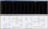
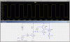
I need to switch a P-chan mosfet on/off (mosfet source voltage will be 9V ...ie a battery) from a PIC pin at about 16Khz - the frequency has to be this high as it'll be in an audio circuit (ie put it above the average adult's hearing) ....a the PIC has a VCC of just 3.3V....therefore the source switching waveform is 16Khz, 0 to 3.3V.

Now clearly, a PIC with a 3.3V cannot turn a P-Chan mosfet whose source is tied to 9V on/off.

So how to get the PIC's output level to be right for switching the p mosfet? At first I thought, just use an n channel mosfet ...gate to the pic pin, source to ground, and a 10k resistor in the drain to 9V...connect the drain/resistor junction to the p mosfet gate .....that will switch between 0V & 9V nicely ...indeed it does, but I don't get a nice square wave on the p chan gate.. it's got typical CR slope thing going on - which means capacitance is creeping in from somewhere - I'm figuring the N mosfet's internal capacitance? (or possibly the p mosfet's gate to source capactiance?)

I tried an digital NPN in place of the fet at q1 - no better!

So what would be the best way to approach this...I don't want to drop the value of the switching frequency ....nor the 10k resistor (ie between the n channel mosfet & 9V as that would really start ramping up the current when the n chan mosfet is switched on (this is destined for a battery fed device).

I'm surprised to be hitting such problems....16khz isnt that high a frequency - there must be a way I can get that p channel gate switched with a nice square wave ?!!

I'd happily buy a proper load switch...but they all seem to be 5V .... I need 9V....also I'd wonder if they'd be any better at 16khz than what I'm experiencing?

**broken link removed**
 
Last edited:
Something like this?
 

Attachments

  • FETdriver.gif
    FETdriver.gif
    22.5 KB · Views: 247
That sounds about right. The gate on a FET is like a capacitor that has to be filled to fully "open" the source-drain. A partially filled gate-capacitance will give a partially-open source-drain, which manifests itself as resistance. So I suspect what you're seeing is the resistance decreasing over time as the gate-capacitance fills up, giving you a non-square signal.

There are two things you have to consider:
1. Most N-chan FETs need more than 3.3V to "turn on". And even if 3.3V is enough, it may not be enough to fully activate the FET. The datasheet should give threshold range. At the lower end of that range, you'll have higher resistances across the FET.

2. The in-rush of current to fill that capacitor needs to be high. Your lowly uC pin can't source more than a few tens of mA. That'll take a long time to fill that gate-capacitance. Which is probably why you're seeing the non-square wave. You can use a BJT as a driver, or buy a driver IC. Anything that can pump a whole bunch of current quickly. IC drivers typically advertise >1A of drive current for that purpose.
 
Last edited:
Why not just use a logic level P-mosfet. The STS5PF20V does pretty good with just 3V gate-source differential.

John
 
I vote with John for the use of "Logic Level MOSFETs". That is what they are designed for.

Ron
 
Why not just use a logic level P-mosfet. The STS5PF20V does pretty good with just 3V gate-source differential.

John

But the p-chan mosfet's 'source' pin is tied to +9v...therefore for the MOSFET to switch, its gate voltage would need to switch between 9v & 6v? (ie 9v minus the 3v threshold) .... or am I missing something here?

By way of an update... I whipped out the P mosfet out of circuit (Q3) ....and replaced the q1 mosfet with an NPN digital tranny .... surprisingly still not that square on the tranny's collector? (i'll post a scope trace in a short while)
 
Last edited:
the gate would need to switch between 9v & 6v (9v minus the 3v threshold) .... or am I missing something?
That's the minimum range required. The circuit in post #2 switches the gate between ~ 9V and ~ 0V and provides a low impedance (= high current) charge/discharge path for the gate capacitance, thus reducing switching time.

Alec, what kind of scope did you use for your post?
That's a screen print from an LTSpice simulation. If anyone wants to run the sim I can post the .asc file.
 
Last edited:
Ok, here's a real world scope trace of a switching signal on the base of Q1 (now a digital NPN tranny)...

**broken link removed**

and here's what the signal looks like on the collector (ugly)...

**broken link removed**

worth underlining - the above traces are for my latest 'stripped back' circuit (Q3 removed), this is all that's in play...

**broken link removed**


Edit: I'm beginning to think this might have something to do with poor PCB track layout (I'm fairly new to board design - & whilst I'm aware of good design practises, sometimes I'm a bit naughty & they've not bit me yet...always a first!) - the stray capactance between the collector and ground on my DVM measures 15nf...which to me seems a lot....and at 16khkz could certainly start impacting slope
 
Last edited:
I have 2 suggestions:

1- make the collector resistor 470 ohms.
2- add some base resistance 1.2k. You probably have something already but 1.2k for the 470 ohm should work.
 
although probably over kill, a simple NPN/PNP totem pole driven by another NPN works nicely for high-side switches, P-channel or otherwise. But of course thats three transistors, instead of just the one :)
 
a simple NPN/PNP totem pole driven by another NPN works nicely for high-side switches, P-channel or otherwise.
.....which is precisely the circuit shown in post #2.

Although the post #2 circuit provides fast FET switching it does gobble current during the pulse edge transients, when both the NPN and PNP are conducting at the same time briefly. By swapping the NPN and PNP positions in the totem pole that transient current is eliminated, at the expense of slower FET switching. Attached are the two arrangements for comparison, plus the .asc file (as requested by Aaron in post #9).
 

Attachments

  • FETdrive2.asc
    4 KB · Views: 139
  • FETdrive2.gif
    FETdrive2.gif
    26.6 KB · Views: 239
Thanks guys...I'll not be able to provide an update until this evening (I live in the UK).

I guess I should lay out my requirements.....I really need whatever switching solution I put in place to be low parts count & low current drain. This is why I used such a high value resistor, because certainly when the N fet was where q1 is, when it's swicthed on that's pure current flowing from the 9V rail to ground.

Therefore with a 1k resistor, that's 9mA when the n mosfet is on - way too much when my power source is a modest 9V battery.

Trutfully, I've not had to deal much with trannies - I realise they amplify current, but how can I work out how much current will flow with a 0 to 3.3V square wave applied to the base ....here's the datasheet ....https://www.electro-tech-online.com/custompdfs/2011/10/0900766b80b36087.pdf (I'm looking for as little current as possible, but to still switch that second p channel mosfet cleanly.)

Also I only actually need the waveform at the P base to swing about 1.5V (therefore 9V applied to the P Mosfet gate = off , 7.5V on its gate = on) ...I guess I could put two resistors in the q1 tranny collector and take the junction to the p mosfet - but that adds a resistor & I'm not even sure if it gives me any win? (from either a clean switching perspective or current drain perspective)

Edit: Hi alec, thanks for your input here (you posted just before me & I missed it) ...I always tend to steer away from stuff I don't understand ...and I don't understand your solution. Actually I don't need to understand it, but I do need to know what the current draw is.....any way of establishing what the current drwa is for say 25%, 50% 100% duty cycle of the switching waveform @16khz? (I have a 'constant current' monitoring situation thing going on with the load .....as the battery levels falls, the 16khz switching waveform duty cycle is increased)
 
Last edited:
but how can I work out how much current will flow with a 0 to 3.3V square wave applied to the base ..
In practice you virtually always apply a voltage via a resistor to the base. As a rule of thumb the base-emitter voltage needed to make a BJT conduct is 0.6V, so if you apply 3V via a resistor R the base current will be (3-0.6)/R amps = 2.4/R amps.
I do need to know what the current draw is..
Do you mean for the whole circuit including the load, or just the driver part up to and including the FET gate?
It's an unfortunate fact that a FET has significant gate capacitance which therefore stores significant charge. That charge has to be moved by the driver part at FET switch on and switch off. The quicker you move it the greater the current. There's no escaping that, so you have to sacrifice speed for current.
 
.....which is precisely the circuit shown in post #2.

Although the post #2 circuit provides fast FET switching it does gobble current during the pulse edge transients, when both the NPN and PNP are conducting at the same time briefly. By swapping the NPN and PNP positions in the totem pole that transient current is eliminated, at the expense of slower FET switching. Attached are the two arrangements for comparison, plus the .asc file (as requested by Aaron in post #9).

Oops! sorry, that'll teach me for not clicking attachments... I just quickly added what I do to switch P-channels - sometimes its not necessary, but I tend to start off 'over doing it' then stripping a circuit down to reduce cost.
 
I have 2 suggestions:

1- make the collector resistor 470 ohms.
2- add some base resistance 1.2k. You probably have something already but 1.2k for the 470 ohm should work.
RonV is right. There is capacitance that the 10k (or 22k) must pull up. T=RC You just have a typical RC time constant.
Capacitance of transistor C-E, C-B, and MOSFET G-S and G-D
 
But the p-chan mosfet's 'source' pin is tied to +9v...therefore for the MOSFET to switch, its gate voltage would need to switch between 9v & 6v? (ie 9v minus the 3v threshold) .... or am I missing something here?
You can shift the level using a capacitor, as shown in the following image.

The minimum gate voltage is 3.3V below 9.6V due to the zener. It's possible to adjust the voltage to 3.3V below the 9V by adding a few parts (resistor, diode, cap).

Note that on startup the gate will be on - a couple of cycles of the drive pin fixes that.
 

Attachments

  • Clipboard01.jpg
    Clipboard01.jpg
    113.1 KB · Views: 197
Last edited:
What FET do you want to use. Lets see what the gate capacitance is so we can see the switching time. How much current will the load take? From the same 9 volt supply?
 
What FET do you want to use. Lets see what the gate capacitance is so we can see the switching time. How much current will the load take? From the same 9 volt supply?

The n-fet I was using was a bss138 (for no other reason, than being readily available!) https://www.electro-tech-online.com/custompdfs/2011/10/0900766b80d22ec5.pdf

The P-fet I was using was a TP0101K https://www.electro-tech-online.com/custompdfs/2011/10/468737.pdf

The load is about 100mA.

What program do I need to get to do those sims?

Also would anyone be able to knock one up for the result I got in my last scope trace (I'd be curious to see what correlation there is)


16kz-> 1k resistor ->NPN tranny base (emitter at ground, collector with a 22k resistor) - scope trace is from the collector


I was quite shocked at the rounding of the square wave with the most simple of circuits wrt my last scope trace that I posted ...and still wonder how much of that 'rounding' is down to pcb intertrack capacitance - therefore a sim would remove that aspect & would help me pinpoint. There's no rounding as the tranny switches on (+ve edge on the base)...the negative headinf slope on the tranny collector is still fairly straight, it's as the tranny cuts off that the 'capacitance' unknown seems to be having an effect?
 
Last edited:
Status
Not open for further replies.

Latest threads

New Articles From Microcontroller Tips

Back
Top