Continue to Site

Welcome to our site!

Electro Tech is an online community (with over 170,000 members) who enjoy talking about and building electronic circuits, projects and gadgets. To participate you need to register. Registration is free. Click here to register now.

  • Welcome to our site! Electro Tech is an online community (with over 170,000 members) who enjoy talking about and building electronic circuits, projects and gadgets. To participate you need to register. Registration is free. Click here to register now.

displaying 2 digits on two 7-segments

Status
Not open for further replies.

abuarab88

New Member
hello everyone,

i hav aproject and i need some hits
w want to design a circuit that displays tow digits from 0-99
on two different 7-segments without using pic microcontroller

the problem is how can we seperate the buttos of the kepad
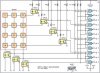
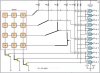
and another help;
the photo in the attached fikes
can any one tell me its purpose and alternatives
 

Attachments

  • untitledbn.JPG
    untitledbn.JPG
    50.4 KB · Views: 154
You need storage for each number. That could consist of a D flip-flop for numbers 0 through nine for each digit (10 flip-flops for each digit). The first set of flip-flop D inputs would be connected to the keypad. The output of these flip-flops would go to the D inputs of the second set of flip-flops.

When the first digit is pushed it will be clocked into the first set of flip-flops (right most digit). Pushing the second digit will clock the first digit into the second set of flip-flops and the second digit into the first set of flip-flops.

The clock for all the flip-flops can be generated by using a 10-input OR gate to detect when any key is pushed. This is a mechanical push button, so you need some type of debounce circuit such as **broken link removed** to avoid generating more than one clock pulse for every push of the button. Since the data will be clocked into the flip-flops when the clock signal goes high you will also need to delay the clock slightly (which would be provided as part of the above debounce circuit) so that the data is stable at the FF input before the clock goes high.
 
To answer your last question, the circuit shown decodes the keypad matrix switch connection to give the 0 through nine plus * and # individual output signals. It also includes opto isolators to electrically isolate the keypad.

If you don't need isolation then you could eliminate the opto isolators. But doing that inverts the signal so you would need to replace the NOR gates in the decoder with NAND gates.
 
The keypad is not electrically isolated; it shares a common power supply. The optos are used to provide voltage translation to drive the logic. The row (top) optos may be removed, while the column (bottom) optos could be replaced with NPN transistors (base to keypad column pin, collector & emitter as per opto C & E), as per attached schem.
 

Attachments

  • untitledbn.JPG
    untitledbn.JPG
    42.5 KB · Views: 132
Status
Not open for further replies.

Latest threads

New Articles From Microcontroller Tips

Back
Top