Continue to Site

Welcome to our site!

Electro Tech is an online community (with over 170,000 members) who enjoy talking about and building electronic circuits, projects and gadgets. To participate you need to register. Registration is free. Click here to register now.

  • Welcome to our site! Electro Tech is an online community (with over 170,000 members) who enjoy talking about and building electronic circuits, projects and gadgets. To participate you need to register. Registration is free. Click here to register now.

Differential Amplifier

Status
Not open for further replies.
Thank you for your patience and time!

hi pm,
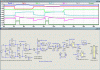
You state that you want to amplify/sample hold/ ADC both the positive and negative signals from the MDL
The requirement for +/- signals will make the design more complex.

So I would propose the following method for your project.

Consider the output from the S/H circuit to be between 0V and +5V , this will drive say a 16bit ADC.

The ADC output will be 0000h for 0V input, which would represent a MDL signal of -50mV and FFFFh for +5V input, which represents an MDL signal of +50mV.

The centre point voltage of +2.5V would give an ADC output of 8000h which would represent an MDL signal of 0mV.

A window comparator at the output of the gain of 50 amp would be set to switch at +/-10mV either side of +2.5V and will generate the S/H pulse.
A set pot will be required to set the threshold voltage.

The S/H pulse will enable a 4066 analog gate connected to the hold capacitor, the output from the cap to the ADC input would be via a non inv buffer amp.

The front end of the main amp would be configured to amplify both pos and neg swings from the MDL sense coil.

The circuits would be powered from a single +12V supply and +5V for the ADC, also a precision +2.50Vref ic.

Look at the circuits already posted and try to configure a new circuit that includes the above features.

OK.
 
Thank you very much for your time.

I figured another way to use the negative pulse. I will place a magnet below the sensor coil so i can reverse the pulse i take.

As a result, i will use the last circuit and test it out.

About the comparator..
Should i use a pull-up or pull-down (with 47KΩ resistor) between 'E' end of basic S&H abd CD4093B or not?
 
Last edited:
Thank you very much for your time.

I figured another way to use the negative pulse. I will place a magnet below the sensor coil so i can reverse the pulse i take.

As a result, i will use the last circuit and test it out.

About the comparator..
Should i use a pull-up or pull-down (with 47KΩ resistor) between 'E' end of basic S&H abd CD4093B or not?

hi,
Why do you think you need a resistor at this point in the circuit.??

Look at this image, its a work in progress circuit that may give you some ideas. Its based on the proposal in my last post.

It needs a little tide up.:)
 

Attachments

  • AAAimage01.gif
    AAAimage01.gif
    33.4 KB · Views: 169
  • MDL3.asc
    6.6 KB · Views: 136
The reason (if there is) is to insure that given no other input, a circuit assumes a default value.

hi,
As the sample generating cct, the 4093 is 'ac' coupled its output always defaults to the low,, disabled state

Is this a college project.?:)
 
Not really.. We had an extra assignment - extra degree, so i tried to do something and maybe i do something on MDL's at later stage
 
Not really.. We had an extra assignment - extra degree, so i tried to do something and maybe i do something on MDL's at later stage

OK,
Lets know how it goes in simulation.:)
 
Hello!

I am a novice at electronics and i have recently started reading about amplifiers and how the gain is calculated(the maths).

So, i search for circuits and try to solve them. I saw the post of pm4698 and there is a scheme (last scheme of page 3) that i tried to solve - calculate the gains of amps till Amp1 end and i stuck.

Could pm4698 or someone tell me how the gains are calculated?The resistors confuse me a lot!

Sorry if the question sounds novice but i am trying to learn so if anyone could answer me i would appreciate it.

Thanx !
 
Last edited:
Hello!

I am a novice at electronics and i have recently started reading about amplifiers and how the gain is calculated(the maths).

So, i search for circuits and try to solve them. I saw the post of pm4698 and there is a scheme (last scheme of page 3) that i tried to solve - calculate the gains of amps till Amp1 end and i stuck.

Could pm4698 or someone tell me how the gains are calculated?The resistors confuse me a lot!

Sorry if the question sounds novice but i am trying to learn so if anyone could answer me i would appreciate it.

Thanx !

hi,:)
Do you mean part of the circuit from page #3.??
 

Attachments

  • AAesp01.gif
    AAesp01.gif
    6.7 KB · Views: 167
hi nick,
I have simplified the circuit and added some formula's.:)

EDIT: corrected typing error in B1a
 

Attachments

  • DiffOPA1.gif
    DiffOPA1.gif
    29 KB · Views: 163
Last edited:
Yes eric i ment this circuit. I will try to solve the simplified circuit and if i have problems i will post here.


Thank you a lot
 
Last edited:
I have two questions.
At the simplified circuit, maybe the A1a = A1 * ......... is A1a = B1 * ......?

and

if there is a Voltage source at the right of the R11 (as at the previous not-simplified circuit) then i will have:

A1a-Vsource = A1 * ...?

Thank you a lot
 
I have two questions.
At the simplified circuit, maybe the A1a = A1 * ......... is A1a = B1 * ......?

and

if there is a Voltage source at the right of the R11 (as at the previous not-simplified circuit) then i will have:

A1a-Vsource = A1 * ...?

Thank you a lot

hi nick,
Well spotted, I had a typing error in the B1 Gain expression, I have corrected the error in the posted image, take a relook.

Sorry about that.:eek:

The purpose of the voltage source in the original circuit was to give the output signal a required offset voltage.

If not used then R11 is connected to 0V.

Please ask any questions.:)
 
nick,

The point to note is that the gains for the non inverting and inverting inputs of an OPA are different.

For the Inv input its G= Rfeedback/Rinput

For the non inv input its G = 1 + [Rfeedback/Rinput]
 
Hi

i would like to inquire about adc for thermocouple. I am designing a temperature data logger whcih needs to meaure up to 350 degree celcius. and the logger should accept J and k thermocouple. can u suggest an ADC which i should use? thanks u very much!:):D
 
Hello eric! I got it how the maths work about the previous post. I took a look at the comparator you have at a circuit at one post. You say that you use that comparator to regulate the control of S & H circuit. How exactly you do this with the CD4093? I saw the datasheet and it shows that is like a NAND gate with Shmitt triggers at the inputs. But at the first CD4093 you have 2 comparators already.
I am mixed up! But i find this example a good Schmitt trigger example and if you have time i would like you to explain it to me (how it works)
I appreciate your help!

hi nickpatsos,
Ref your PM.:)
Which circuit,,, Amp200c or MDL3...???
 
It is the circuit at page 3 (you have attached an MDL3.asc file there) and its the part from Amp1 to first S & H circuit
 
It is the circuit at page 3 (you have attached an MDL3.asc file there) and its the part from Amp1 to first S & H circuit

hi,
I have edited the MDL3 and added text for the different functions.

Look it over, ask any questions.
 

Attachments

  • MDL3sh1.gif
    MDL3sh1.gif
    39.7 KB · Views: 134
I searched for the CD4093 datasheet to see how it works and i read that is consists of 4 NAND gates with 2 inputs with Schmitt trigger function to each input. I read also that a Schmitt trigger is actually a comparator.So...
1)The high/low comparator is for the Schmitt trigger function or not? If not, why do you use the comparators?
2)How can you make the NAND gate to operate as an OR Gate or as an invertor as you write at later stage of the circuit?
3)What do you mean about high edge diff?

I appreciate your help!
 
Status
Not open for further replies.

Latest threads

New Articles From Microcontroller Tips

Back
Top