hi
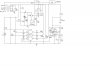
In my circuit I had a 230/12. rectified, and filtered(using 470uF), supply which supplies an electrmagnetic relay of 12v 200 ohms. taking approximately 80 mA.
Now I need to tap 5.1 V, 9.1 V and 15V from the same source, for which i used Zener diodes. 5.1V zener is for charging 4700uF Capacitor. 9.1V is for 555timer and 15V is for IC4011. Accordingly what are the resistors to be used?
I used 10k resistor for each zener. Is it OK?
also, From pspice i found that filtering capacitor(470uF) power dissipation is having around 15 watts pulses. why is it so?
")
")
