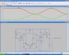
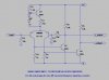
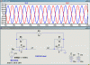
I'm making a tri-output signal generator, the last stage of which is a triangle to sine wave convertor. I have the stage working and generating a nice sine wave, but I want to drive it with a differential signal. The attached circuit is intended to accept the single-ended tirangle wave, and produce a differential triangle wave to drive the convertor. The voltage driving the amp is identical to the signal I'm presently generating in the 'real' version ( linear trialgle wave from +4Vmin to +8Vmax )
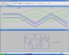
Clearly, I have a problem in that the differential driver is easily driven into the non-linear region, Q1 being driven into cutoff. There are several solutions available to prevent this.
1) Increase the value of R5
2) Adjust R9/R8 voltage divider
3) Implement feedback (R4 to Q2 base)
Either of these solutions would work well for simulation. Does anyone have an opinion what would work best for real devices?
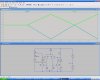
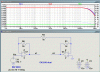
Waveform Guidance
Red: Source Voltage
Blue: Q1 Collector Voltage
Green: Q2 Collector Voltage
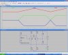
Clearly, I have a problem in that the differential driver is easily driven into the non-linear region, Q1 being driven into cutoff. There are several solutions available to prevent this.
1) Increase the value of R5
2) Adjust R9/R8 voltage divider
3) Implement feedback (R4 to Q2 base)
Either of these solutions would work well for simulation. Does anyone have an opinion what would work best for real devices?
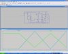
Waveform Guidance
Red: Source Voltage
Blue: Q1 Collector Voltage
Green: Q2 Collector Voltage
Attachments
Last edited:
")