Continue to Site

Welcome to our site!

Electro Tech is an online community (with over 170,000 members) who enjoy talking about and building electronic circuits, projects and gadgets. To participate you need to register. Registration is free. Click here to register now.

  • Welcome to our site! Electro Tech is an online community (with over 170,000 members) who enjoy talking about and building electronic circuits, projects and gadgets. To participate you need to register. Registration is free. Click here to register now.

DC Power Supply circuit - additional strange parts

Status
Not open for further replies.

steven7890

New Member
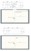
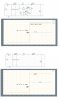
Hi all, I got the power supply circuit diagram from internet, I understand this is a dual DC O/P (+5V and +12V) used in home appliances. But I can't figure out the function and operation of Q1/Q2/R31 for +12V. Also the D15/C30 for +5V. Could anyone please help to advise? Many Thanks :happy:
奇怪的电源电路 1.jpg
 
Hi,

It would help to know what this circuit was designed to power.

With a quick viewing of the Q1 / Q2 circuit, it looks like the normal load requires current limiting which is provided by the 10 ohm resistor in that circuit. But the load may need a higher current to start properly so the transistors are added. Their function would be to allow a higher current pulse to get through during the startup phase when the circuit is first turned on.
It is a little puzzling why the two caps to ground are so low in value however, so it would really help to know what it is powering. Maybe it would help if we knew where you found this circuit.

The other diode D15 and cap dont make any sense.
 
Either there is a mistake in the drawing, or the original poster doesn't have a clue...

There are lots of questionable things posted on the Internet.

Post your link to the circuit.
 
I copied the above schematic from this China web address **broken link removed** . It is a technical internet forum for home electric appliances. The one posted this diagram did not mention the actual application and the load type of this strange power supply. And no one in the forum could provide a logical explanation for Q1 and Q2. I did simulation to see the difference with and without the Q1+Q2+R30+C26+C27 when connecting a resistive load, plus a capacitor (switched in at a later timing) to see how it handle sudden surge load current. And their results show no difference at all.
I am now pretty sure that this schematic is truly questionable, as mentioned by Mike. Another evident to support this doubtful circuit is D15 + C30 which an experienced designer should never do that. We are waiting our time here, sorry
 

Attachments

  • Strange Power Supply simulation 1.jpg
    Strange Power Supply simulation 1.jpg
    622.7 KB · Views: 189
Hi,

I never waste my time. I thought the circuit was at least a little interesting anyway :)

I told you what Q1 and Q2 would probably do and the operating mode they would affect, but you tested it for some other mode of operation and came to the conclusion that it does not do anything when really what you concluded was that it does not do anything for THAT particular mode of operation. You wont be able to see what Q1 and Q2 do unless you test it properly.

Q1 and Q2 will mostly affect the TURN ON transient of the ENTIRE circuit, not just the turn on of the load. In fact, it probably wont do much for the load transient.

So to test this properly you've got to start with a resistive load, and DC input, and turn the DC input on suddenly.
At the very least it can be used for a slow start circuit, although there are probably better ways to do that.

You can also test it with larger cap values to see what you can get it to do. In some cases you can probably get it to allow a larger current flow to the load during the turn on transient time.
 
One questionable thing is that a TIP42 can apparently be both a PNP device and an NPN device !
 
Aren't they both clearly drawn as PNP?.
Oops! Must remember to put glasses on.
 
(1) the circuit of Q1+Q2+R30+C26+C27 is effectively in "parallel" with R31 (10 ohm) and lie between the power source and the load, so there is no way to limit the inrush current with a parallel topography.
(2) the circuit of Q1+Q2+R30+C26+C27 could help to deliver large start-up load current during that transient time. I'm also very doubtful it could work. Because to do that Q1 must be able to deliver large current from its corrector to the load. And to order to make this, firstly it needs a large capacitor at its emitter (not 0,1uF , C26), secondly its "base-emitter forward bias voltage (Vbe of Q1)" or "base current" must be there. But I dunt see these in the schemtic. Anyway. I will do another simulation and let you people see

Note that my simulation posted are using 10uF for C26, its result is very much the same as 0.1uF
 
Could the circuit of Q1+Q2+R30+C26+C27 could help to deliver large start-up load current during the transient time ?
Please see the attached simulation results, the first one is with the suspicious circuit. The DC power supply 19V and SW1 is switched on at 0.1 second. The second one is without the circuit. However their results are almost the same. This shows that the effect of Q1+Q2+R30+C26+C27 in the said power supply schematic is nothing or worthless....
 

Attachments

  • Strange Power Supply simulation 2.jpg
    Strange Power Supply simulation 2.jpg
    528.3 KB · Views: 187
Hi steven,

Now try it with a resistive load.
 
Only resistive load (10 ohm) now is under simulation, see attached. Again I compared with and without the circuit of Q1+Q2+R30+C26+C27 to check their difference upon power on (DC). But I still dunt see the effect of the said cct of the Q1+Q2+R30+C26+C27......:banghead:
 

Attachments

  • Strange Power Supply simulation 3.jpg
    Strange Power Supply simulation 3.jpg
    505.2 KB · Views: 174
Hi,

Now try different cap values like 1uf, 10uf.
 
Only capacitive load (1uF and then 10uF) is simulated, see attached. Again I compared with and without the circuit of Q1+Q2+R30+C26+C27 to check their difference upon power on (DC). But again I dunt see the effect of the said cct of the Q1+Q2+R30+C26+C27......
 

Attachments

  • Strange Power Supply simulation 4.jpg
    Strange Power Supply simulation 4.jpg
    942.9 KB · Views: 172
Hi,

Yeah, you seem to want to see this circuit fail to perform any action at all. Every time i suggest a test you manage to change something that makes it appear to not do anything. The only thing strange to me is why you are doing this.

With the larger caps and resistive load you'll see what it does, ANY other way and you WILL NOT be able to see what it does.

With circuits who's behavior is unknown we strive to understand how they work, and to do that we have to devise tests that will bring out the functions that the circuit can perform. We dont just test with whatever conditions we feel like testing it with, we try to find out which ones will show how it does or could work.

There are many reasons for wanting to do this, the most obvious is to find out how exactly it works and when it works. If we can not find anything then maybe the designer made some small error or did not draw the schematic correctly so there may be some small modification we can make to get the circuit up and running, and with flying colors :)

Your goal should really be to find out under what conditions it will work or what small modification might be made to get it to work. If you discard it too soon you might miss something great :)
 
My goal is to check what Q1/Q2 can contribute in this simple power supply circuit. I did some simulations myself ( I have shown one of them in above), and rather sure Q1/Q2 could not make any difference to the circuit performance. You are the one thought that Q1/Q2 could help in start-up inrush load current, so I cooperated with you to make 3 simulations and eventually concluded that Q1/Q2 again failed to show any benefit at all. The results were not inline with your expectation, clearly I know. Nevertheless, my goal is met, Q1/Q2 configuration is surly a crap, from a guy who even put a diode in series with a capacitor (D15/C30). If you still like to go further with it (to find out under what conditions it will work), by all means please proceed in your side.
 
Hi,

Well the circuit does do something and you'll never know what it is simply because you refuse to do the simulation the way i described, and it even seems like you went out of your way not to do it in the prescribed way. So dont use it then. When i try to help someone with a circuit and they go out of their way to try to make it fail, i'm pretty much done with it.

In the end it's up to you whether you want to use it or not, so if you are so sure of your conclusion then your only logical continuation is not to use it :)
 
After few simulations, one with basic knowledge of BJT transistors (+ other basic components ) should logically know how the crap circuit of Q1/Q2 behave without simulating all the possibilities (in fact it is almost unlimited possibilities) and make good and logical conclusion. And this is what I have done. Furthermore I havealready made clear not to trust someone who even put a diode in series with a capacitor (D15/C30). So again you may want to proceed further, go ahead.
 
Status
Not open for further replies.

Latest threads

Back
Top