Continue to Site

Welcome to our site!

Electro Tech is an online community (with over 170,000 members) who enjoy talking about and building electronic circuits, projects and gadgets. To participate you need to register. Registration is free. Click here to register now.

  • Welcome to our site! Electro Tech is an online community (with over 170,000 members) who enjoy talking about and building electronic circuits, projects and gadgets. To participate you need to register. Registration is free. Click here to register now.

Cybernetic Data Products LED Sign (circa 1980’s) Memory Backup

Status
Not open for further replies.

Vons Garage

New Member
Issue: Device will not store messages after power off.

Good day.
ADT3100 LED Sign - Overview of Device.JPG


This LED sign is touted as having “a rechargeable battery for memory backup … for at least 3 months”. As there are zero batteries in this thing, near as I can figure they are using a 17,000 mfd cap as the “rechargeable” battery. This part was recently replaced and still no memory storage.

You guys are the pros. Can a 17,000 mfd cap allow an RCA CDM6116E2 CMOS 2048-Word by 8-bit LSI Static RAM keeps it’s programming for 3 months?

Or were the sales team and manual writers thinking of a future unit; perhaps the one that member “slywuf” inquired about back in 01/29/2019? That sign looks way different than my fellow. And I can see a great big Panasonic battery on his motherboard, wear as mine has the cap wired-in way back prior to the power supply.
ADT3100 LED Sign - Overview Comments.jpg


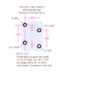
And for future reference; I have included a manual that I rewrote for this sign for those that may find it handy.
 

Attachments

  • Adver-tiser Owners Manual - FINAL - PDF Convert.pdf
    1.7 MB · Views: 257
It's hard to know, with nothing to compare it against, and no idea what changes might have been made to it over the decades.

It's quite likely the battery was removed to prevent damage - they have a fairly short live and commonly pour corrosion all over the board.

The 17,000uF looks to be a reservoir, not backup - the two bodged on sideways caps on the main board look suspicious to me. Presumably the 6116 is what needs backing up?.
 
This takes me back to the 1980. I designed one of these for a company in Michigan (USA).
I had a battery on the back side the board.
I see a mixture of low power CMOS and high power logic ICs. So I don't see how the entire board can stay powered from a capacitor.
The RAM is the only memory that can store the information when power is lost. Unless there is something I can't see. Is there a real time clock on board?
I had two diodes on the power pin of the RAM. RAM got power from the main 5V or from the battery which ever is higher. I can not find diodes in that area. It is possible that one of the capacitors holds up the RAM supply only. With time the capacitor is leaky and can not do it's job.
-----------------------------------
I looked at the data sheet for the RAM. If everything is right it will pull 50uA. (assuming everything is powered down) at room temperature, a voltage regulator will need to be working.
 
Last edited:
Well my first computer was a Microtan Tangerine kit, which I still have, and I expanded it into a rack case with back plane and various plug-in extra boards, including a monochrome graphics card, AND a battery backed RAM card. The RAM card was paged on the back plane, as was the graphics card and various others in the 65K 6502 address space.

While it's not been used for a number of decades, I just had a quick look - as I remembered the battery backed RAM card is full of 6116 CMOS chips and a (rather leaky looking) NiCd battery.
 
So nice to hear from you fellows. Thanks.
No visible signs of leaky stuff - but - Mr. Goodwin got me thinking and, sure enough, something pulled from the PCB from who-knows-when.
IMG_0450.JPG

IMG_0449.JPG

Any suggestions on which pin number I should trace back from on the RAM chip and see if it heads anywhere near the cap and/or the empty pads on the PCB? And perhaps hazard a guess on the battery (NiCad or sure) voltage and capacity values? Maybe I can zoom in the other fellows version of this device posted on this cool site and see the Panasonic nomenclature. Maybe their engineers stayed with the same scheme on Ver.2
1628519416916.png
 
Trace back from pin 24 on the RAM - that's where it must have power to retain data.

The item removed appears to have powered the 4093 (centre top, upper picture) which being CMOS could well be part of the backup control logic, to disable the RAM write or CE whilst on battery power.
 
RJ; Traceback drawing below. Will poke around the PS PCB next and see what's on connector P2 / Pin #1.
Doesn't seem promising. Pin 24 on the RAM gets nowhere near the empty holes on the PCB where I really am now starting to think are the pulled NiCad's. Very strange geometry on the NiCad pin layout. Not symmetrical.
Nigel; thank you. I will look around further and see if this backup scheme may be hiding on this board.
Pin #24 traceback - foil view.jpg
Pin #24 traceback.jpg
 
Interesting - the middle pin of that three pin header appears to go to the battery? object that was removed, fed via a copper link and a resistor.

The third looks to go to other inputs on the 4093, via a resistor and the pot next to it?

It may be that the board was designed for an alternate off-board backup device, as well as the onboard option.

Do you get any voltage on the two used pads for the removed bit, when it has power on? I'd make a wild guess that it may originally have had a three cell NiCd or NiMH pack using the four pads, so roughly 3 - 4.5V range.
If it was and the charge circuit has not been disabled it should show something like 4.5 - 5V when on power.
 
RJ;
I will pursue your observations. Only two of the four "pads" from the suspected battery pack are active in the circuit. The other two were for hold-down of the pack. I will poke around and provide a bunch of voltage reading and will continue to trace power flow on PCB photos. More marked up photos coming. Stand by my friends and thanks again for following along and sharing your expertise.
UPDATE: Chart of voltages taken at P2 Power Inlet. Numbered from right-to-left as you view the component side of the PCB.
UPDATE: NiCad pads measure +5.02 / -0.03 when powered up.
UPDATE: All voltages on P2 die immediately upon power off. The 17,000µF cap ain't doin' diddly squat.
Next up:
1) Dimensions of NiCad pad area just in case someone recognizes this strange pattern. DONE - thumbnail
2) Pull the power supply PCB and draw that schematic. Started - 1st time drawing a schematic from a PCB - MUCH harder than I thought.
3) Draw out the "Master Power" and "Display ON/OFF" switching circuit. It's a real head-scratcher.
Or maybe I should just buy a APC UPS and be done with it.
ADT3100 LED Sign - Incoming Power Volt - JPG Convert.jpg
 

Attachments

  • Battery BU Dimensions.jpg
    Battery BU Dimensions.jpg
    205.2 KB · Views: 230
Last edited:
Update and Close:
Photos of power supply were traced and schematic attempt of this two-sided PCB just made me more confused. The pads that rjenkinsgb steered me to did not have any "ah-ha" insight when probing for voltages.
I gave up.
Thanks all for trying to help.
 

Attachments

  • Power Supply - NOT DONE.pdf
    99.9 KB · Views: 202
Status
Not open for further replies.

Latest threads

New Articles From Microcontroller Tips

Back
Top