Continue to Site

Welcome to our site!

Electro Tech is an online community (with over 170,000 members) who enjoy talking about and building electronic circuits, projects and gadgets. To participate you need to register. Registration is free. Click here to register now.

  • Welcome to our site! Electro Tech is an online community (with over 170,000 members) who enjoy talking about and building electronic circuits, projects and gadgets. To participate you need to register. Registration is free. Click here to register now.

Combination Lock, Understanding.

Status
Not open for further replies.

Karkas

Member
Hello, I have this project attached and i was trying to understand its whole operation and got stuck.

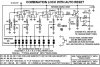
They're using 4 D-type FFs, and the number of the combination are connected to the Clock inputs, and the data input of the first Flip Flop is connected to GND, so that at the first clock pulse it is reset and its Q output is connected to the Data input of the second Flip Flop so the same happens with the second FF when the Clock input is given by the combination, and continues with the other flip flops, so if the right combination is provided there will be a LOW in the Q output of the last FF, and the transistor is cuttoff because of the specifications in theFF datasheet, it says that it will provide 8.8 mA in the output when it's LOW and using 15V of Vdd, and that's what i dont' understand, why if I give the right combination the transistor will be cuttof? the solenoid won't be activated. By the way, i don't have very much knowledge about solenoids, maybe its operation is not that obvious and that's why i don't understand.

The opposite happens if you enter a wrong combination, because all the other switches are connected to the SET inputs, and no matter the state of the DATa input or the CLOCK it will be HIGH at the Q outputs, and that will turn on the transistor because it will provide -8.8 mA in that output, that means 8.8 mA flowing from outside to inside, right? and that will saturate the transistor, it complements my missunderstanding explained above.

Maybe the right transistor is an NPN, only a guess.

Another question i have is:
What would be the first state of the flip flops before the first Clock pulse is given? SET right? i mean What impedes that i only give the last number of the combination and reset the last flip flop and un lock the system? necesarily a SET i guess.

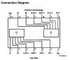
The connection Diagram of theFlip Flop is also attached.
Thanks.
Hope you help me understand this.
 

Attachments

  • Combination lock picture.JPG
    Combination lock picture.JPG
    68.5 KB · Views: 981
  • D-type FF.JPG
    D-type FF.JPG
    17.8 KB · Views: 625
Last edited:
The circuit seems to be a successful design but you can do all this with one 8 pin PIC chip. You can change the code to anything you want and it will provide "lock-out" of 5 minutes after 3 incorrect tries.
It will also have debounce on the switches and LEDs to show when a correct code has been entered and it only requires 4 buttons marked A,B,C and D. Pushing A, C, C, D will turn on the "ok, door open" LED and then you push A and D at the same time for the length of time you want the solenoid or actuator to operate. Any of these features can be changed to anything at all by adding your own code to the program.
The microcontroller project will cost less than the project above and will be much more reliable. LEDs on the project will indicate "fail" "insert new code" "enter code" - this LED will be illuminated all the time when the circuit is activated, to show it is ready to receive an entry code and the fourth LED will be "ok, door open" When all LEDs flash - lock-out for 5 minutes. These LEDs will not be visible on the 4-button display - they will be on the PC board and can be placed anywhere to help you enter the code and insert a new code.
 
Last edited:
I would have to agree with colin, some type of debouncing on the switches would be a must.
 
The circuit does not need debouncing of the switches as the D flip-flops are wired so that they either flip or flop when a HIGH is entered via the clock line (pins 3 and 11).
At the beginning of the sequence, the reset line going to pins 6 and 8 SET the flips flops to the SET condition in which the Q output is HIGH (pins 1 and 13).
The wiring of the circuit makes pin 5 and 9 HIGH and in this condition pin 3 and 11 will have no effect on the output.
But the first flip flop has pin 9 LOW so pin 11 will make pin 13 go LOW when it (pin 11) goes HIGH.
Pin 13 of the first flip flop is connected to pin 5 of the second flip flop and it is now LOW, so that a HIGH on pin 3 will make pin 1 go LOW.
This action is repeated with the third and fourth flip flop and finally pin 1 of the fourth flip flop goes LOW to activate the solenoid.
The activation of the four flips flops must start at flip flop 1 as a flip flop cannot change state until pin 5 or 9 is LOW.
 
Thanks, i can see the idea but happens that, I don't program microcontrollers yet, I apreciate your ideas and if I programmed microcontrollers I would take it, but I don't yet, I'm going to take the Digital Systems Lab class next semester wich is actually beginning next week and once I aprove it I will be able to take Microprocessors, by now I would really apreciate any help you can provide with the questions I posted, and if you can add it some information about where I can find some tutorials or maybe something deeper, maybe books, or anything about microcontrollers and the programation software, which ones are best and the languages, so i can get started in that because i'm very interested.

Thanks.
 
Last edited:
Thanks I understand that, but why a LOW in the pin 1 of thelast Flip Flop will activate the solenoid, it will provide an aproximated 8.8mA and that will cut-off the transistor, is that the requirement for the solenoid the be activated?, then I'll have to ask why?
Also, I can't see why at the beginning they are SET.
 
The project must be kept in the "reset" condition so that the solenoid is not activated. In this project, the “reset” condition happens to be the condition when the flip flops are in the SET state.
In the SET state, the output of the fourth flip flop has a HIGH on pin 1 and this means the base and emitter of the PNP transistor are at the same potential and the transistor is NOT turned on.
The voltage on the base of the PNP transistor must be taken towards the 0v rail by an amount of about 0.7v less than the 12v rail to turn the transistor ON. In other words about 11.4v and this is done by creating a LOW on pin 1 of the fourth flip flop and the resistor R11 will drop the difference in voltage between the output of the flip flop and 11.4v on the base. The base cannot go lower than 11.4v and so the resistor allows about 11v to appear across it and according to the value of the resistor, a current will flow and the amount of current can be worked out by Ohm’s Law.
The chip will only allow about 8 – 15mA to flow and the size of the resistor is chosen so that the current is within this range.
The transistor will amplify this current about 70 – 100 times and this is the maximum current that will flow in the collector-emitter circuit – and thus through the solenoid. The resistance of the solenoid will determine the actual current and if it is less than the current worked out above, the circuit will work successfully. In addition, the type of transistor used in the circuit will determine the actual maximum current.
We are just saying the chip will allow 8 x 100 = 800mA to flow in the collector circuit and the transistor and solenoid can be selected for this current-flow or preferably a lower current.
 
Look, i couldn't understand what you said about those voltages in the transistor, in the datasheet of the Flip Flop says:
Output Current for LOW:

for Vdd=10V, Vo=0.5V, Io=2.25mA. the positive current indicates that it is coming out from the output, right?

for Vdd=15V, Vo=1.5V, Io=8.8mA.

And when they're HIGH they have the same current but with a (-), that means they are demanding that current in the output right?

So, what I see is that if the pin 1 is HIGH (SET) they Flip Flop has -8.8mA (suposing that i'm using Vdd=15V) and if it demands a current of 8.8mA from a PNP transistor base it will be turned ON ar very probably in Sat. And the opposite happens if the pin 1 is LOW.

About what you said about those Voltages, Can't see it, because if pin 1 is HIGH using Vdd=15V voltage pin1 will be 13.5V, and will be demanding a 8.8mA current, and the base will be at
Vin output - V in 1k5 resistor, i'm not so sure about that, but I don't understand why you say that the base will be at the same potential than the emitter, the emitter will be at Vdd, but even if i'm wrong in that about the voltage in the base, i don't think the base will be at Vdd.

I'm using Vdd=15V just because of the especifications, and for not seeing what you say about the voltages. and other thing, the chip, won't provide or demand that current in the specifications indepéndently of the resistor in the output, right? I thought it was that way, but by reading what you say:

The chip will only allow about 8 – 15mA to flow and the size of the resistor is chosen so that the current is within this range.

So, if it's so, then i'm getting more confused. I hope you explaime that to me.
Thank you very much.
 
Last edited:
Forget about what you read in the datasheet. It only confuses you.
When a 4000 chip is HIGH, the output can supply about 8 - 15mA when the supply is 12v. The 4013 is one in this CMOS range.
When the output is LOW, the line can sink about 8 - 15mA.
This is all you have to remember. I try to make things simple for you.
When the chip is connected to a 12v rail, the maximum output voltage will be about 11v - 11.5v and the minimum voltage will be about 0.5v when the output is LOW.
 
Ok, i'm trying to forget it, but also in the Digital Systems textbooks i learned that in CMOS when outputs are LOW the have greater current than when they're HIGH and it's generally is 0 or negative.

Thanks for trying to make things simple, but if I keep things in my mind like that, how could I respond when somebody comes to me with an issue like this, i will only be able to give simple answers and not only because i'm trying to make things simple, but also because that's all I know.

What I would like is to understand de difference between what i read in the datasheet, and the Digital Systems book, and what you're saying, because it must be the same or there's something really important that i'm missing, the i would understand the functioning of the circuit.
 
Yes. The low current capability can be greater than the high current capability. The low voltage will always be slightly higher than 0v and the high voltage will always be slightly less than rail voltage.
You are just beginning. Once you build hundreds of circuits using these CMOS chips you will able to venture into understanding some of the data you are trying to grasp.
But if you make one slight slip by saying something like: the output will go below 0v rail; all the high-fallutin’ knowledge in the world is not going do you any good.
 
But if you make one slight slip by saying something like: the output will go below 0v rail; all the high-fallutin’ knowledge in the world is not going do you any good.

Excuse me but I didn't understand that, surely because of the language, but now that we're saying the same thing bout the Iol and the Ioh, you can explain me that about 8.8mA when low and -8.8mA when high, don't care about the magnitude, just the - or +, was I wrong about what I said about demanding or providing?

That could be a good beginning.
 
This thread has not expired yet, in case somebody can still hep me.
 
Status
Not open for further replies.

Latest threads

New Articles From Microcontroller Tips

Back
Top