Continue to Site

Welcome to our site!

Electro Tech is an online community (with over 170,000 members) who enjoy talking about and building electronic circuits, projects and gadgets. To participate you need to register. Registration is free. Click here to register now.

  • Welcome to our site! Electro Tech is an online community (with over 170,000 members) who enjoy talking about and building electronic circuits, projects and gadgets. To participate you need to register. Registration is free. Click here to register now.

Christmas Star project

Status
Not open for further replies.
Visitor. I had a slight error in a gerber file, one solder pad for a edge connector had no solder mask (to expose copper). JLCPCB noticed my error and paused production to ask if that is what I intended. I said "no" and offered to send a corrected gerber - they said I didn't have to, they corrected it for me. Amazing service for the price. My total order (multiple designs) was over $150 but that prototype PCB was only a 5 piece, $2 order.
 
I realize how small the parts are. ALL the LEDs (0603's) on top layer to be assembled.
Bottom layer with pic and 1203 resistor arrays, I will assemble.
Main reason is aesthetics. I have about 20- 18f43K22 pics and my next plan is a Seahawk head with green eyes. How would it look with a bunch of tiny parts on the face?
This is ART mixed with electronics.
And yes I tried placing the pic at a 45 degree angle but it worked out better as I pictured it (left,right,top,bottom.
I placed LEDs according to same pin out.
Hopefully will get boards ordered this week. With all the smoke, can't go outside.
 

Attachments

  • sea hawk pic.jpg
    sea hawk pic.jpg
    79.2 KB · Views: 208
Just trying to help you have a successful project.

I know I don't enjoy soldering tiny parts when I have the option of letting somebody else do it.
 
I kinda enjoy soldering but not even going to attempt anything smaller than 1206.
My wife even mentioned that I seem to enjoy assembling boards.
When I get the board ready to submit maybe I can send you the gerber to look over?
 
When I get the board ready to submit maybe I can send you the gerber to look over?

I'm kind of reluctant to do that, because I don't want to be responsible for any issues their might be.

If (a very big if) I did that, I'd want to look at the schematic and board files, not the Gerbers. I would only be willing to look once, at the absolutely final, no more changes version, and I've accept zero responsibility, blame, guilt or anything else if there turned out to be a problem. I've made enough of your problems my problem. See for example this entire thread.
 
The plan has never changed, A star with LEDs on the front only. Everything else on back.
Started out with everything on front but really never happy with components other than LEDs on front.
finally have the board laid out, needs some cleaning up of crocked traces etc. then need to make the silk screen the inverse image so only the white outline is printed. Did a board that was supposed to be all one color and had the front with copper area on front and the board came back with a silver front. Didn't want the silver.
Screenshot (11).png
 
If the entire layer was solder-coated copper, the layer you put on the front was soldermask, not silkscreen.
 
Just looking in the area of the USB connector, a number of less-than-ideal things come up.

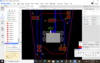
1. The USB connector is pointing up, so the cable will come in from the top. I don't think this is what you intended. Also, there doesn't seem to be mounting pads for the ears that hold the connector to the board.

Hmmm. Maybe this is a vertical connector instead of right angle (haven't seen one in SMT), which means the cable would exit perpendicular to the board....which will likely rip the connector off the board. Also, if this is the case, rotate the connector 180 degrees to fix the routing.

2. The V+ trace from the USB connector is too close to the mounting pin. Correcting the orientation of the connector will solve this.

3. The power for all the LEDs goes through the V+ trace from the USB jack. I suggest (again) that it be a big wide track,

4. There's an "interesting" jog in the track to the right of the connector.

5. Put the vias for the LEDs a little farther away from the pads. Vias too close to SMT pads can lead to assembly problems.


Sorry. I am way too picky about board layout to review your board. Doing so would drive me insane (granted, it might not be a long drive at this point!).

EasyEDA - MrDEB USB 1.jpg


EasyEDA - MrDEB USB 2.jpg
 
will make corrections as suggested. The +5v trace is .500 wide. Maybe go wider?
I want the usb connector pointing down (will investigate)
 
That doesn't match what's on the board picture you posted. This connector is a MINI-B while the one in the picture you posted is a FULL-SIZE B.

Are you trying to say you switched to this? A MINI-B is a really poor choice as it has been deprecated (i.e., removed from) the USB standard. It's the least rugged of the USB connectors, is obsolete and cables for it may be difficult to locate.

You either want a full-size B connector, for which long cables are readily available) or micro-B, which is widely used. No USB-C as it will be impossible to hand solder.


I would make your power trace 1 or even 2 mm wide, then narrow it down near the micro. Bigger is better in this case and with all those LEDs, this trace could be carrying a lot of current (I can only guess at how much because you keep changing every-damn-thing so you don't know what you've got and anybody following along hasn't a clue.
 
I changed the usb connector but keep getting drc errors
part # is C40940 or C40958
either one gets DRC errors?
 

Attachments

  • Screenshot (13).png
    Screenshot (13).png
    242.8 KB · Views: 239
  • Screenshot (14).png
    Screenshot (14).png
    243.7 KB · Views: 255
Sorry Charlie,

You need to look at the datasheets. Both of those connectors mount in a cutout at the edge of the board. They will not work placed in the middle of a board.

Depending on the settings in the design rules, on fine-pitched components, you may get a clearance error. Understand what "errors" can sometimes be ignored.

Screenshot_20200920-143137_NokoPrint.jpg
Screenshot_20200920-142950_NokoPrint.jpg
 
Notice the big square in the middle of the footprint? That's a cutout in the board. It must go at the edge of the board, and the connector body is between the top and bottom of the board.

EasyEDA usb footprint.jpg
 
Well looks like I am maybe a "NO SMT ASSEMBLY" unless a green star is ok.
Just might have to use 1206 leds on top layer OR hope that I can solder either 0603 or 0805 LEDS
one heck of alot of LEDs or cover the leds with grease. then spray paint the boards blue.
covering with grease would be maybe the easiest route.
NOTE: smt assembly ONLY on green boards. Asked JLCPCB
 
Status
Not open for further replies.

Latest threads

New Articles From Microcontroller Tips

Back
Top