Continue to Site

Welcome to our site!

Electro Tech is an online community (with over 170,000 members) who enjoy talking about and building electronic circuits, projects and gadgets. To participate you need to register. Registration is free. Click here to register now.

  • Welcome to our site! Electro Tech is an online community (with over 170,000 members) who enjoy talking about and building electronic circuits, projects and gadgets. To participate you need to register. Registration is free. Click here to register now.

Christmas Star project

Status
Not open for further replies.
any suggestions on avoiding the solder mask? Yes all I did was lay down traces, never occurred about solder mask.
 
The most obvious solution is to find the proper footprint for the SMT connector you have.

Or just use a regular through-hole pattern, but only populate it on the board you use to develop code. On the others, just put a header in the position when you want to load code and tip it at an angle to get good contact when you dump the code in.
 
discovered how to make traces into pads
first I only had 2mm wide short traces
then click on the trace/ convert to pad/ expand the solder mask
 

Attachments

  • Screenshot (1).jpg
    Screenshot (1).jpg
    178.2 KB · Views: 194
part # I have is from Mouser #M20-7910542R
made by Harwin
data sheet say pads are 2.54 ctr to ctr 1mmW x 2mmT
 
So, you have two options:

1. Design a footprint from the datasheet. All the dimensions you need are there.

footprint 1.jpg


2. Mouser provides the symbol and footprint in a universal format. Download the file, follow the instructions to convert it to Eagle 7 format, and import into EasyEDA. In this case, drawing it vs importing it may be a wash, but for a more complex part, understanding how to import it saves a lot of time and trouble.

footprint 2.jpg


Download the file and the library loader program. Follow the instructions and import into EasyEDA.


footprint 3.jpg
 
THAT Samacsys program is really helpful. Have it on the startup menue.
Have board almost complete but that copper pour is an issue when I found two traces that need to be put on bottom layer.
Maybe just redo the copper pour.
 

Attachments

  • PCB_copy1 pcb_2020-09-03_09-13-06.pdf
    249.1 KB · Views: 207
Traces on the bottom ground plane are fine, along as they don't cut the ground plane in two.

Press [shift] R to rebuild the ground plane when you add traces on that layer or move anything.
 
You might try the following settings to to post pictures of your board.

It will be a little easier to see what's going on. Saving as a PNG will result in a directly viewable picture here.

EasyEDA Board Export.jpg
 
will give it a go BUT discovered a new issue after I reload changes then check errors it says VIA DIAMETER
I have the via set at min via diameter of .6 (should be fine after I looked at the board requirements with a hole size of .3
doing something really wrong?
 
It depends on parameters that are set in the program. It should be fine, but why push the capabilities of the fab house when there's no need to. I usually set general vias to 0.8mm dia, 0.4mm drill, and set my trace width to 10mils (0.254mm) unless there is a compelling reason not to do so.
 
am discovering lots of errors on the board after I SAVE > RELOAD NETS> DRC ERRORS
The bottom shows several rat lines still.
I have a via next to each LED for ground.
Needs more work IMO
 
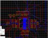
Many of your LEDs have a via next to them, with no connection to the pad on the top layer. Other LEDs have no connection to the ground pin at all.

Your power trace from the USB connector needs to be far wider. Remember, every LED is fed from this trace. Too wide is never an issue. Too narrow, if you turn on a bunch of LEDs and you may glitch the micro
 
the last board picture was #2 in design. Have saved under copy#3
Will post another pic later. Just doing some minor part adjustments and looks like I need to change the USB connector from type B to a type C.
 
Status
Not open for further replies.

Latest threads

Back
Top