Continue to Site

Welcome to our site!

Electro Tech is an online community (with over 170,000 members) who enjoy talking about and building electronic circuits, projects and gadgets. To participate you need to register. Registration is free. Click here to register now.

  • Welcome to our site! Electro Tech is an online community (with over 170,000 members) who enjoy talking about and building electronic circuits, projects and gadgets. To participate you need to register. Registration is free. Click here to register now.

Can I add a FET in parallel to this boost circuit

Status
Not open for further replies.

DarrenB

Member
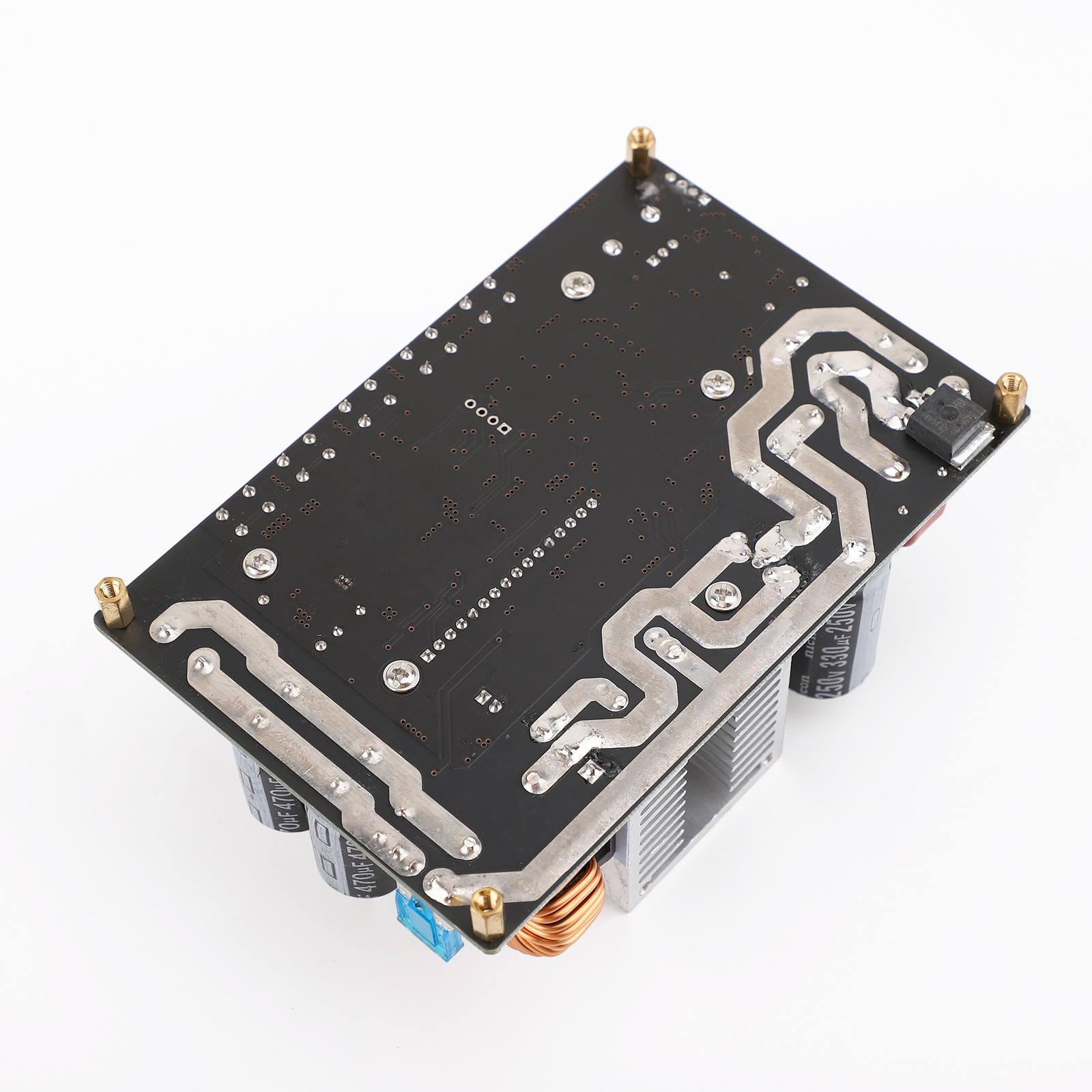
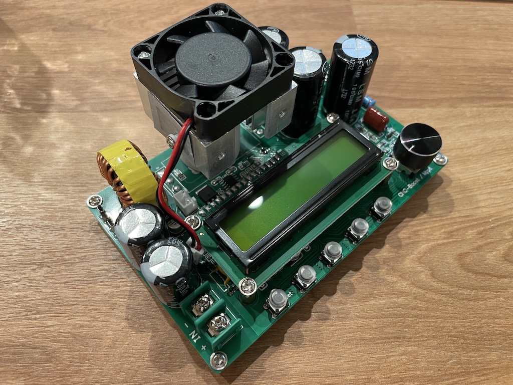
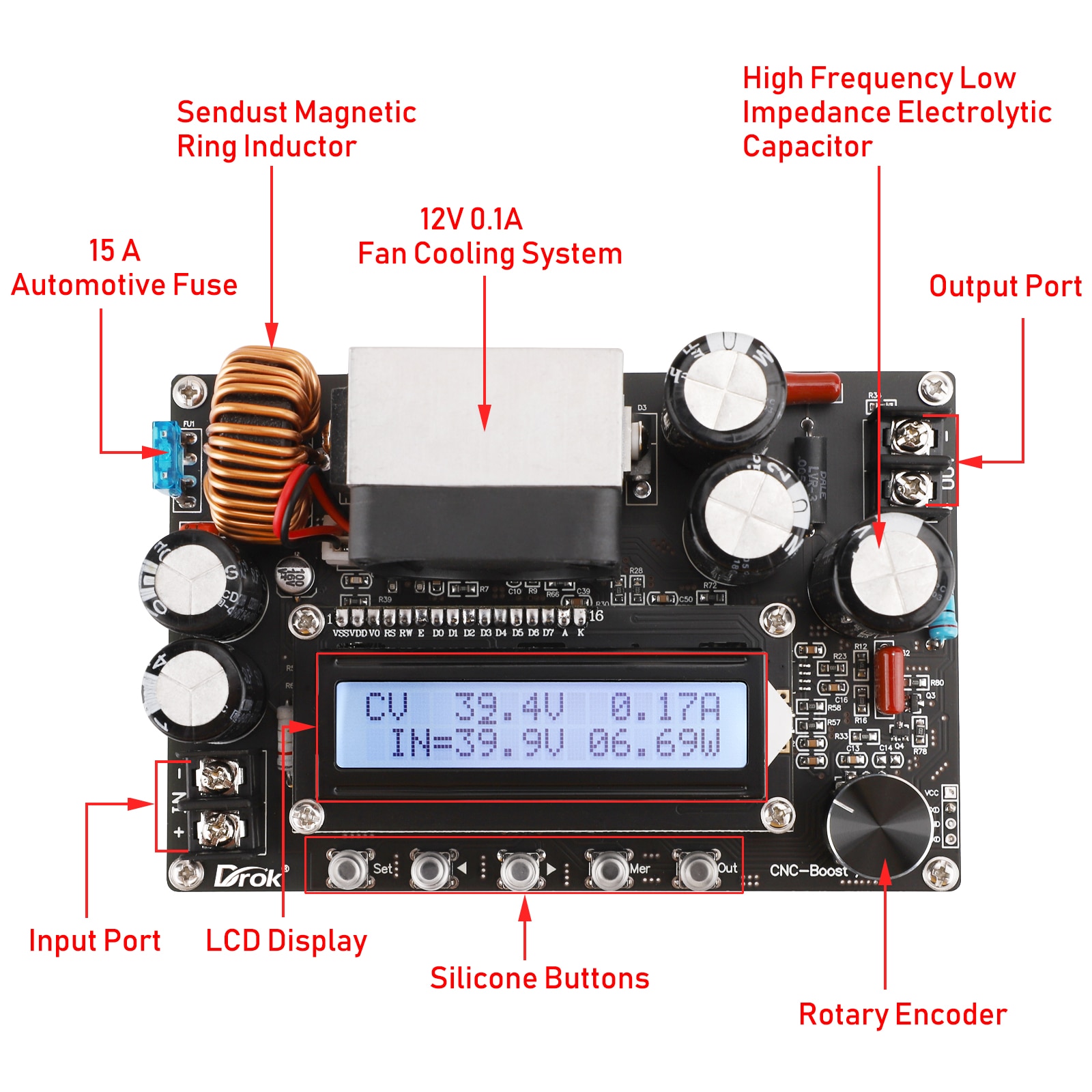
I use these AliExpress boost converters to charge batteries but I would like to make it function closer to its rated specifications. At the moment it gets really hot when at around 70% of its max rated load. I have tried replacing the fan with one that has a higher static pressure rating and it helped considerably but I was thinking I could take it further by adding a larger heatsink and another FET in parallel. Is it possible to add an identical FET in parallel to this pre made boost converter? It currently uses a 055N15A but If possible I would replace it with 2x IRFP4568. I know that the total heat will equal roughly the same but I am more concerned the thermal path being larger and the heat being shared across two packages. I am a complete beginner when it comes to electronics so please forgive me if this is a stupid question.
Boost 4.JPG
Boost 1.jpeg
Boost 2.jpeg
 
I don't use fets/mosfets, but i guess it's the same for bi-polar transisters. So yes, you will need low resistance resistors on each source pin.
 
It would probably make it even worse...

A common problem with cheap devices using large power FETS is the circuit not having enough gate drive current, so the power device does not switch as fast as it could - and it's when it is part on that the power dissipation is very high.

The existing device has a typical gate capacitance of 7.1nF and maximum almost 9.5nF

The IRFP4568 are rated 10.5nF typical. Having double that is going to slow the switching far more & mean the FETs waste a lot of power.

ps. The module is apparently a "DPX800S"


What input & output currents & voltages is it running at?
Thank you for such a well explained reply. I haven't got one of these modules with me now but I will try and find the gate driver part number.

I use these modules at all voltages and currents within specifications, wattage and temperature. I would like to be able to get a bit closer to the 15A input and 800W output. I used to use the trusty old house brick boost converter (as pictured) in a printed case with 2x 92mm fans and it was really reliable. The heatsink temperature never really went over 40C. I recently changed over to the DPX800S because it has a display and is digitally controlled. I miss having the 20A input so I would like to get closer to the 15A rating on the DPX800S.
IMG_0258.JPG
Boost 3.jpeg
 
Remember the output limit is 10A; you can only [theoretically] achieve 800W at over 80V output.

At less than 80V, the wattage max is 10A x o/p volts, by the makers spec.

What input and output voltages are you using?
 
Remember the output limit is 10A; you can only [theoretically] achieve 800W at over 80V output.

At less than 80V, the wattage max is 10A x o/p volts, by the makers spec.

What input and output voltages are you using?
I use it at various voltages but mostly 12V, 36V and 52V on the input.
Also of concern is gate drive R typically used to suppress parasitic L
transients, eg. its Pdiss. Make sure that R has sufficient power handling
capability.


Regards, Dana.
Once I have the module with me I will post the pn for the gate driver. Do you know of any mosfet I can get that is better than the 055N15A, maybe I could use a single fet which has a lower resistance rather than using two?
 
The dissipation due to "on" resistance at 30A (eg. 15A average at 50% duty cycle) is near enough half a watt, half the time - so a quarter watt; near enough irrelevant.

All the heat is due to dissipation while it is changing between fully off and fully on.

Something like one of these may actually work better, as it's got reasonable current and voltage ratings, but much lower gate capacitance, so should switch faster:
 
I don't use fets/mosfets, but i guess it's the same for bi-polar transisters. So yes, you will need low resistance resistors on each source pin.
Bi-polar transistors do need resistors to balance their current, but MOSFETs have a positive temperature coefficient for their on-resistance so will inherently tend to share the load current when used as switches, no source resistor needed.
 
If relying on Rdson matching of paralled MOSFETs w/o ballasting I would be
concerned with this -

1657588272685.png


Looks like a significant current non sharing in the making.

And typically since multiple MOSFETS typically in the same thermal environment
they all experience similar heat rise, mitigating some of the beneficial effect of
rising Rdson with T. Not to lose full insight this is all non linear and starting at different
points on the Rdson vs T curve for each device I would still want to swamp out that variation
with ballasting unless I match at device test.

A crude sim of the problem -

1657591932025.png


Regards, Dana.
 
Last edited:
Bi-polar transistors do need resistors to balance their current, but MOSFETs have a positive temperature coefficient for their on-resistance so will inherently tend to share the load current when used as switches, no source resistor needed.
So on a BMS which has multiple mosfets I don't need to try and place the cable in the centre of them? I always thought this would help spread the load but from what you are saying they do it themselves due to their positive temperature coefficient?
The dissipation due to "on" resistance at 30A (eg. 15A average at 50% duty cycle) is near enough half a watt, half the time - so a quarter watt; near enough irrelevant.

All the heat is due to dissipation while it is changing between fully off and fully on.

Something like one of these may actually work better, as it's got reasonable current and voltage ratings, but much lower gate capacitance, so should switch faster:
Thanks. I'll grab some temperature data from the stock setup then buy one of the mosfets and re measure. I used to think the main specification on mosfets was the rdson but it makes sense that the gate capacitance is extremely important. Most of the things I have that use mosfets are all power converting. Edit: I just checked and TK56A12N1 is in a TO-220 package? Will the heat transfer negate the gains or will it still be worth it? I assume there is nothing in a TO-247 package that is available at the moment. I can source the TK56A12N1.
If relying on Rdson matching of paralled MOSFETs w/o ballasting I would be
concerned with this -

View attachment 137793

Looks like a significant current non sharing in the making.

And typically since multiple MOSFETS typically in the same thermal environment
they all experience similar heat rise, mitigating some of the beneficial effect of
rising Rdson with T. Not to lose full insight this is all non linear and starting at different
points on the Rdson vs T curve for each device I would still want to swamp out that variation
with ballasting unless I match at device test.


Regards, Dana.
I am guessing this is referring to the crutschow post? Ballasting = resistors? Are you saying that because the mosfets are generally within close proximity of each other on the PCB it is still a good idea to use ballasting? What is ballasting?
 
Last edited:
Ballasting in this context is to insure MOSFETs that are paralleled, when on,
one of them do not hog most of the current thereby overloading it. So one
adds R in series to mitigate device to device Rdson variation and Vth varia-
tion where one turns on before the others. crutschow is correct, there is a
+ tempco to Rdson such that when MOSFET has more current it heats up and
its Rdson mitigating some of the current rise effect, eg. negative feedback.
But one has to do analysis to see if that effect insures no device is ever over
its ratings due to all changes such as initial Rdson tolerance, board layout
(slight R changes in traces), etc.. In fact in RF work this becomes very important
for RF Power MOSFETs because of all the AC parasitic involved resulting in RMS
power differences between them. Note also Rdson variation with T is non
linear, complicating analysis even more.

So at high currents using low Rdson MOSFETs one adds R in series to lessen the
effect due to simple load sharing differences. The sim I showed shows this problem,
but not a complete analysis as the device specs only show a typical and max Rdson
value, no minimum, so the worst case is not handled, eg. one MOSFET at minimum,
one at maximum, for the analysis.

Simply think of the problem as a simple voltage divider effect with load and the
paralled R's, and accounting for all tolerances.

Lastly note ballasting at high currents typically done with trace length versus
discrete R's.


Regards, Dana.

PS : By the way many high power MOSFETs actually have internal ballasting due to
their architecture. To insure no hot spots developed on die. You can google that.
 
Last edited:
So it's best to over spec the mosfet and use resistors or design the trace to accompany the mosfets. How do you work out the value of R or is it just a generic value?
Ballasting in this context is to insure MOSFETs that are paralleled, when on,
one of them do not hog most of the current thereby overloading it. So one
adds R in series to mitigate device to device Rdson variation and Vth varia-
tion where one turns on before the others. crutschow is correct, there is a
+ tempco to Rdson such that when MOSFET has more current it heats up and
its Rdson mitigating some of the current rise effect, eg. negative feedback.
But one has to do analysis to see if that effect insures no device is ever over
its ratings due to all changes such as initial Rdson tolerance, board layout
(slight R changes in traces), etc.. In fact in RF work this becomes very important
for RF Power MOSFETs because of all the AC parasitic involved resulting in RMS
power differences between them. Note also Rdson variation with T is non
linear, complicating analysis even more.

So at high currents using low Rdson MOSFETs one adds R in series to lessen the
effect due to simple load sharing differences. The sim I showed shows this problem,
but not a complete analysis as the device specs only show a typical and max Rdson
value, no minimum, so the worst case is not handled, eg. one MOSFET at minimum,
one at maximum, for the analysis.

Simply think of the problem as a simple voltage divider effect with load and the
paralled R's, and accounting for all tolerances.

Lastly note ballasting at high currents typically done with trace length versus
discrete R's.


Regards, Dana.

PS : By the way many high power MOSFETs actually have internal ballasting due to
their architecture. To insure no hot spots developed on die. You can google tha
 
Last edited:
So it's best to over spec the mosfet and use resistors or design the trace to accompany the mosfets. How do you work out the value of R or is it just a generic value?
He's vastly overcomplicating things for you - just stick a pair of identical FET's in parallel, with heatsinks etc. and see how hot they get, compared to a single FET. Bear in mind, you're still dissipating the same amount of heat, just spread across two FET's and heatsinks.
 
He's vastly overcomplicating things for you - just stick a pair of identical FET's in parallel, with heatsinks etc. and see how hot they get, compared to a single FET. Bear in mind, you're still dissipating the same amount of heat, just spread across two FET's and heatsinks.
To be honest I like to learn anyway. What you're saying makes things extremely easy though as sharing the heat load is the goal I am trying to achieve and measuring the amount of heat is directly linked to the resistance or performance/efficiency when they are in parallel. I think I will post the pn for the gate driver just to make sure as I don't want to buy another batch of mosfets as mousers shipping is ridiculous. Rjenkinsgbs suggestion of the TK56A12N1 seems like a good idea to be honest. Is it possible to deliver more current into the gate to achieve the same effect, I know it would be easier to change the mosfet but I wondered if it is possible to do that with a different gate driver? Also would using 2x TK56A12N1 be silly or overkill?
 
To be honest I like to learn anyway. What you're saying makes things extremely easy though as sharing the heat load is the goal I am trying to achieve and measuring the amount of heat is directly linked to the resistance or performance/efficiency when they are in parallel. I think I will post the pn for the gate driver just to make sure as I don't want to buy another batch of mosfets as mousers shipping is ridiculous. Rjenkinsgbs suggestion of the TK56A12N1 seems like a good idea to be honest. Is it possible to deliver more current into the gate to achieve the same effect, I know it would be easier to change the mosfet but I wondered if it is possible to do that with a different gate driver? Also would using 2x TK56A12N1 be silly or overkill?

Yes you can always throw parts into a design and burn them up, thats a positive learning
experience. Or take reasonable well established principles and protect in advance as the
posted ap notes show from the experts. Good engineering generally does the latter. Of
course you can always check the "identical" box when you order parts. let me know who
will ship to that precise spec.....:)

Regards, Dana.
 
Last edited:
As I see it, spreading the load across two transistors and two heatsinks can only help. 'If' the FET isn't switching fast enough, then increasing gate current will help - but it all depends on how 'slow' it might be, and if the difference is great enough.
 
Yes you can always throw parts into a design and burn them up, thats a positive learning
experience. Or take reasonable well established principles and protect in advance as the
posted ap notes show from the experts. Good engineering generally does the latter. Of
course you can always check the "identical" box when you order parts. let me know who
will ship to that precise spec.....:)

Regards, Dana.
I can't. These modules are already really fragile and shorting them blows nearly everything else on the PCB leaving them uneconomical or too difficult to repair. Unfortunately though I do not know enough about electronics to be able to make a better decision other than a guesstimate. This is why I ask in places like here because you guys are clearly way more experienced in this subject. Any advise is always appreciated!

I will post the part no for the gate driver and then hopefully you can let me know which mosfet/mosfets will be best to use as an upgrade.

As I see it, spreading the load across two transistors and two heatsinks can only help. 'If' the FET isn't switching fast enough, then increasing gate current will help - but it all depends on how 'slow' it might be, and if the difference is great enough.
I will post the pn for the gate driver and then it should hopefully be clear if swapping out the 055N15A for something with a lower gate capacitance will help. From what the other guy said it doesn't sound like it can be anything else as 1/4W certainly isn't what it is turning into heat. Hopefully he is right and it makes a noticeable difference. I wonder why they didn't figure that out and use a fet with a lower gate capacitance in the first place though.
 
Equally important is board layout to minimize transients and timing alterations.

There are ap notes on this, and books on SMPS that discuss this in detail.


Good test instrumentation, such as a DSO, say 50 Mhz or better, very prudent to evaluate
signal integrity, transients, etc..


Regards, Dana.
 
I have tried reading through things like this before but each and every hurdle will spur another question. I think I need to understand the basics of electronics. Electronics is a bit like a puzzle for me where the more you learn the easier it becomes. It can also be a bit like having a missing critical part to a math equation :(. Understanding what the values on data sheets are and how they interact with one another would probably also help. How did you learn electronic engineering? Self taught or an education program?
 
Status
Not open for further replies.

Latest threads

New Articles From Microcontroller Tips

Back
Top