Quick idea on an envelope. lol
From computer or FPGA. (A, B) Digital data 0/5V could be 0/3.3.
Transistor changes 0/5V to = -5V/0V. Level shifter.
IC1 is simple buffer (could be inverter)
IC2 is also simple buffer BUT the supply is connected to 0V and the "ground pin" is connected to -5V. (output is 0 and -5V)
I chose resistors to get near 50 ohms. Could choose higher values. (if 3.3V supply you will need to change the 680 resistors.
AB=00= -0.35V if I did the math right.
AB=11= +0.35V
AB=01 or 10 you will get 0V.
View attachment 107861
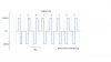
There are other ways. Maybe 30 different ways. You will need to update the outputs every 2uS.
p.s. looks like I did not do the math right. (voltage divider, 5V to 0.35V, simple math for some one awake)(resistor to +5V and resistor to ground, the third resistor is in parallel with the 56 ohm resistor)