Hi,
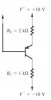
I dont know what level of detail you are looking for here, but in some problems when the base is open then the collector base current becomes a deciding factor on what the transistor is doing. The collector base leakage is always present, but you would have to look at the data sheet and temperature to determine if the current is turning on the transistor a little. To compensate for this, most transistor circuits have a resistor from emitter to base so that this leakage current is swamped out. With the resistor, the leakage current is not high enough to reach the turn on threshold voltage of the base emitter.
If the base is connected directly to +10v in this circuit, then all the leakage current is forced into the +10v supply line and the transistor would be considered completely 'off' in most cases.
This could be an exercise to show the difference between having an open base and a base that is connected so as to shunt all leakage current bypassing the emitter base.
Look up the data sheet, then decide what you think about the leakage current specification. If you dont have a part number, trying using a common PNP transistor part number.

")