Continue to Site

Welcome to our site!

Electro Tech is an online community (with over 170,000 members) who enjoy talking about and building electronic circuits, projects and gadgets. To participate you need to register. Registration is free. Click here to register now.

  • Welcome to our site! Electro Tech is an online community (with over 170,000 members) who enjoy talking about and building electronic circuits, projects and gadgets. To participate you need to register. Registration is free. Click here to register now.

ADC conversion clock?

Status
Not open for further replies.

Pommie

Well-Known Member
Most Helpful Member
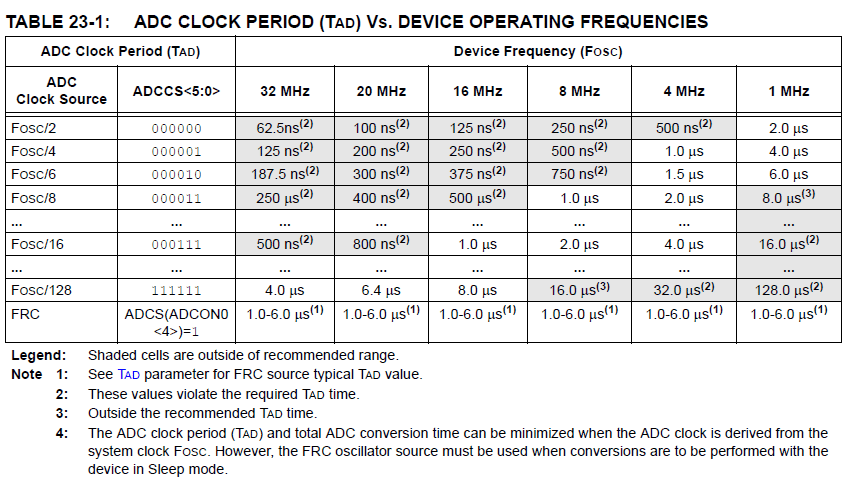
I'm using one of the newer Pic16 series chips and the ADC has become a lot more complex. However, the writers of the datasheet seem to have gotten lazy. In this table they've skipped a lot of rows (I think),
ADC1.png

The way I'm reading the above is that 1.0uS is a good period for TAD. I'm running at 32MHz and assume that there's a missing row of Fosc/32 where my time will be 1uS.
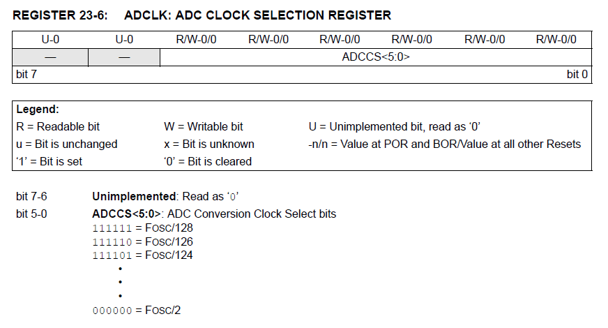
To further confuse the matter, the register where you set this value seems to have a typo,
ADC2.png

Surely those (divisor) values should be halving each row and Fosc/124 is a typo and should be Fosc/32?

Is there another document that describes this?

Thanks for any comment.

Mike.
 
Perhaps just use the MCC to set it up, then cut and paste the setup code to your own application.
I keep having to setup a dummy project so I can do just that. Oh well, that's a job for in the morning.

One interesting thing I've found with PPS is that is you put a CCP or PWM output on a pin you can no longer use it as a simple I/O - it's PWM (or capture) only.

Mike.
 
I keep having to setup a dummy project so I can do just that. Oh well, that's a job for in the morning.

I tend to set a dummy project up and return to it if I'm using the same device, and add any extra settings - then cut and paste.

One interesting thing I've found with PPS is that is you put a CCP or PWM output on a pin you can no longer use it as a simple I/O - it's PWM (or capture) only.

Mike.

Yes, if you allocate a peripheral to an I/O pin you have to unallocate it to use it as an I/O later.

I do a lot of low power stuff, and if you're using UART's the TX pin is high by default - so when you enter sleep mode current flows out the TX pin killing your low consumption.

Shutting the UART down doesn't help, so I found the answer is to shut the UART down, reallocate the TX pin elsewhere via PPS, and then with the TX now a standard I/O set it low. On waking from sleep, do the reverse.
 
To further confuse the matter, the register where you set this value seems to have a typo,
View attachment 127585
Surely those (divisor) values should be halving each row and Fosc/124 is a typo and should be Fosc/32?

Is there another document that describes this?

Thanks for any comment.

Mike.
I don't see anything wrong with the table. The divide ratio is 2 * (ASCCS<5:0> + 1)

The 6 bits of ASCCS<5:0> read as a binary number in the range 0 - 63
Adding one gives 1 - 64
Multiplying by 2 gives 2 - 128

If you want to divide by 32, ASCCS<5:0> should be 15 or 001111
 
I don't see anything wrong with the table. The divide ratio is 2 * (ASCCS<5:0> + 1)

The 6 bits of ASCCS<5:0> read as a binary number in the range 0 - 63
Adding one gives 1 - 64
Multiplying by 2 gives 2 - 128

If you want to divide by 32, ASCCS<5:0> should be 15 or 001111
You are, of course, correct. Guess I got confused due to the top table going in binary steps and assumed the bottom table was a typo. Morning here now, let's see if a clearer head helps me to get this working.

Mike.
 
Status
Not open for further replies.

Latest threads

New Articles From Microcontroller Tips

Back
Top