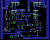
Continue to Site

Welcome to our site!

Electro Tech is an online community (with over 170,000 members) who enjoy talking about and building electronic circuits, projects and gadgets. To participate you need to register. Registration is free. Click here to register now.

  • Welcome to our site! Electro Tech is an online community (with over 170,000 members) who enjoy talking about and building electronic circuits, projects and gadgets. To participate you need to register. Registration is free. Click here to register now.

About make an audio power amplifier.

Status
Not open for further replies.
Comments:
The pads to the external world don't look evenly spaced. May not allow a connector to be used. The pads may be too small.

If this was a commercial board ans even if it wasn't, it's hard to tell which resistor is R5 and R6.

So, move the silk screen stuff a bit:
Center NTC with respect to R2
Move the labels R5 and R6 so you can tell which is which.
The BC557 is way out in right field.
Center R3 and R?
You can move the labels Q2 and TIP41C
I'd use a square PAD on one of the legs of C1 (I can't remember what the common convention is), probably negative. That's the striped side,

I think, "T" corners should be avoided. I think that's an etching issue.

If your etching this yourself, put some sort of label on the component side in copper, so you know what side is up. You don't want to etch a mirror image, Trust me.

One leg of R4 doesn't go anywhere?

Last, but not least. There are no mounting holes.
Thanks a lot. But any problem with T corner? Mounting holes for what? NTC thermistor will be attach to the heatsink directly.
 
See here: https://electronics.stackexchange.c...reference-for-45-degree-angles-in-pcb-routing point #9.
Really it isn't that important.

The missing trace on the 68K resistor is the most important bug.

OK, so you don't need mounting holes, Consider this scenario. Let's say you place 4 mounting holes in a rectangular pattern. Before stuffing the board, use 4 standoffs. Insert the lowest components while on the standoffs, the turn the board over to solder and clip. They do provide an "extra hand" during assembly and the board is easier to grip when you turn it over. A more complex board might benefit for troubleshooting. Your choice.
 
A more complex board might benefit for troubleshooting.
Yep, big boards like power amp or preamp with need mounting holes.
Debugged version:
c0oler.PNG

The space behind TIP42 back is for small heatsink.
 
No autorouters, especially in the low end ECAD packages, are pretty dumb.
Yes, I am think so. Only a very simple circuit that I can draw directly to the copper clad board but the program made very dump layout.
I presume that is a layout for an audio amplifier.
Yes, this is a layout for Elliott P3A 100W amp which we discussed.
The way I use to arrange parts in the board is aped from Elliott PCB:
**broken link removed**
 
My PCB layout, please point out mistake or given me advices: :)
TIP3055 and TIP2955 just for same pinouts with actually NJW3281 and NJW1302
100W OCL.png
 
Last edited:
Comments:
If you were having this made, it probably would not be accepted. The copper should not go to the edge of the board.
Label the inouts, output and + and - supplies.

I found it useful to put an RCA phono connector on my amp board. I also used a pigtail to a Molex connector for power, speaker and ground.

Not sure if the mounting screws being part of the ground is a good idea. It, sort of, defeats the idea of a star ground.
 
The copper should not go to the edge of the board.
This problem can be solved easily.
Label the inouts, output and + and - supplies.
I don't need to silk screen printing.
I found it useful to put an RCA phono connector on my amp board. I also used a pigtail to a Molex connector for power, speaker and ground.
I use this connector in PCB surface:
bo-cam-han-6.jpg

Not sure if the mounting screws being part of the ground is a good idea. It, sort of, defeats the idea of a star ground.
I don't think it will connect to the chassis, I have PP cylindrical washers.
 
I don't need to silk screen printing.


True. But for your own documentation, it would be worth it.

FWIW: I did some really nice boards with Easytrax (DOS and obsolete) software and my own etching. I used polyester paper and a printed that glued to the board with 77 spray adhesive.

==

The audio input is special in way. You want the shield to terminate close by. You can't do that with the connectors you chose. I'm only referring to the audio input. Phono is also the same as the actual input. It just made troubleshooting easier.

As I said earlier, I could remove my AMP PCB and troubleshoot with an extension cable(s). I lost a few things when I did, but nothing serious.
 
The audio input is special in way. You want the shield to terminate close by. You can't do that with the connectors you chose. I'm only referring to the audio input. Phono is also the same as the actual input. It just made troubleshooting easier.
My connectors only for power supply and audio output. The audio input will have RCA connectors PCB mounts.
FWIW: I did some really nice boards with Easytrax (DOS and obsolete) software and my own etching. I used polyester paper and a printed that glued to the board with 77 spray adhesive.
I think I will go for an iron, eraser and water.
 
Although I haven't checked each trace, this looks like a good layout- well done.

spec
 
Your pcb shows the very old 2N3055 and 2N2955 transistors used in my amplifier that I still use. It is 52 years old.
 
This is no more complicated than a discrete UA741 Op Amp, it is only a 6 stage design with parallel complementary circuits and parallel output stage and differential input. Extra Q's are for crossover distortionless balanced feedback bias (Q7,10,11) and current limiters Q8,9. Thus only 6 gain stages with good linearity and low output impedance from differential stage feedback with output. Zout is reduced by feedback gain so you have a nice low output impedance to pump speaker coil without load fluctuations of moving coil forcing distortion on power signal source, like a battery or ideal voltage source.

That being said.,Building a 741 op amp from discrete parts is complicated , but necessary to provide the voltage or in this case power gain needed with good linearity.

ESR of supply caps must be <0.1% of speaker coil reistance for low distortion and ripple which is brute force way of regulating voltage and ripple distortion. So choose design quality over simplicity for best results.
 
10% distortion of HF signals with 30 Hz bass power is easy to fix with more parallel output stages and more gain feedback. ( but excess gain and stages can cause oscillation which is why snubber RC dummy loads are often included)

1% distortion is common in most consumer cheap amps.
0.1% distortion is possible with high quality designs at max power.

you decide what you want.
 
To go from std 1V line 10K input to say 50V with an ouput impedance equivalent of 1% of typical speaker coil resistance of 2Ohms or Zout<20 milliohms requires your supply impedance to be equally low ,which often demands 50W diode ratings (ESR~=1/W rating) even though you would never dissipate that much.

this implies a theoretical "matched impedance" power gain of from 10k input to 20m output with a voltage gain of say Vcc-diode drops of a few V determined by several feedback R ratios. eg. R37:R28 for + side and (R17+18):R19 both polarities.

Since gain and bandwidth products tend to be constant, lower voltage gain increases power bandwidth. In this case a power Amp (without preamp) has a low voltage gain typically 100 more or less. But more important, a Power Amp has massive current gain, hence 6 stages with current shared outputs with fairly well matched devices. (xx3055 devices are around hFE=50 at high current.).
To reduce output impedance of say 1Ω to 20mΩ the voltage open loop gain is reduced by some R ratios to yield a same reduction in low frequency (low pass filtered) output impedance needed specifically for large moving coil woofer speakers.
The Leach Amp reduces 10k input to nearly 20mΩ output impedance implying an impedance reduction of 500,000. The actual current gain impedance depends on speaker minimum impedance which will be slightly higher than DC R of coil and average impedance depends on other physical properties like cone area and coil force with magnetics and current might be 4 or 8Ω for standardization.

Another way to think of the job of this impedance reduction as the necessary design factor is often defined by "Dampening Factor, DF" which is simply the impedance ratio of speaker to Amp output impedance , where >100 is desireable and >1000 is possible in commercial power amps. This is inverse to load regulation where we know if load is is same as series source , voltage drops 50% and 1% distortion might occur worst case if 1:100 impedance ratio or DF=100. And ideal power source has zero Ω but is impossible to achieve even if powered by a nuclear reactor.

I hope you reread until you understand or ask someone to explain better
 
Your pcb shows the very old 2N3055 and 2N2955 transistors used in my amplifier that I still use. It is 52 years old.
I don't want to create 2SC3281 and 2SA1302 (I am so lazy) so I used TIP3055 and TIP2955 as templates because they have the same pinout and distance between each pin. Of course I will not go for TIP3055 and TIP2955.
 
I don't want to create 2SC3281 and 2SA1302 (I am so lazy) so I used TIP3055 and TIP2955 as templates because they have the same pinout and distance between each pin. Of course I will not go for TIP3055 and TIP2955.
Just check that the pin spacing of the transistors that you are using are the same as the TIP3055/TIP2955. Some output transistors are TO247 etc. For future experiments (transistor rolling) it would be advisable to cater for all likely cases on the PCB. But it is not a big deal because you can always adapt the leads of a power transistor to fit the PCB- just a bit tidier and electrically better.

spec
 
Status
Not open for further replies.

Latest threads

New Articles From Microcontroller Tips

Back
Top