Continue to Site

Welcome to our site!

Electro Tech is an online community (with over 170,000 members) who enjoy talking about and building electronic circuits, projects and gadgets. To participate you need to register. Registration is free. Click here to register now.

  • Welcome to our site! Electro Tech is an online community (with over 170,000 members) who enjoy talking about and building electronic circuits, projects and gadgets. To participate you need to register. Registration is free. Click here to register now.

80C51 code not working

Status
Not open for further replies.

mstechca

New Member
I can program my EEPROM through the parallel port, and the data appears to be stored on it. I have verified the 1st byte manually.

Now when I use the same EEPROM in my 8051 circuit, and turn the unit on, all I see on my HD47780 compatible LCD is a bar filling half the display, If I make the RESET pin high, for a few seconds, and make RESET low, the same bars start flickering at a very high rate.

The code is as follows and works with my compiler.

Code:
mov P3,1
MOV P1,63
clr P3.0
setb P3.0
MOV P1,15
clr P3.0
setb P3.0
MOV P1,1
clr P3.0
setb P3.0
setb P3.1
MOV P1,"H
clr P3.0
setb P3.0
MOV P1,"E
clr P3.0
setb P3.0
MOV P1,"L
clr P3.0
setb P3.0
MOV P1,"L
clr P3.0
setb P3.0
MOV P1,"O
clr P3.0
setb P3.0
MOV P1,"!
clr P3.0
setb P3.0

The above code is the same as the 8051 instruction set except that:

any parameter starting with a quotation mark instructs the compiler to give the ASCII equivalent of the character after the quotation mark.

clr means clear bit.

P1, P2, P3, and P0 refer to the respective ports.

The least I expect the system to do is clear the display, and it can't do that.

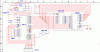
My circuit is included, and the little red lightning bolts are shown, because Windraft (the schematic editor I was using) expected me to connect the pins (with the bolts) somewhere.

Someone please tell me what I am doing wrong.
 

Attachments

  • frame1_174.gif
    frame1_174.gif
    15.5 KB · Views: 972
You appear to have the 28C64 connected to be always readable (/OE low, /CE low /WR high). When you then try to write A0-A7, wont the data (of the eprom) lines fight with the port lines when you try to write to the 74HC245 latch? I.E. Port (8051) and Data (2864) are both outputs at the same time.

Mike.
 
I just realised, the 245 isn't even a latch. I've now no idea how that circuit is supposed to work.

Mike.
 
have u initialised the LCD in the proper manner.??ie settings all the control registers?
Yes

You appear to have the 28C64 connected to be always readable (/OE low, /CE low /WR high).
I intend to have P0 and P2 set exclusively for the address pins and data pins of the EEPROM, and nothing else.

When you then try to write A0-A7, wont the data (of the eprom) lines fight with the port lines when you try to write to the 74HC245 latch?
I.E. Port (8051) and Data (2864) are both outputs at the same time.
the 74HCT245 latch has 2 sets of 8 I/O lines, an inverted enable line, and a send/receive line.

The send/receive line is forced to 1, so that data flows from port A to port B on the 74HCT245 latch. The ALE on the 8051 is connected to the inverted enable line through an inverter, so that when ALE is high, the latch is enabled, and the address ports become active.

I took 1/2 my circuit from alot of websites. The only changes I made were:

- using the 74HC245 (and an inverter) in place of the 74HC373
- tying read and chip enable lines low


I just realised, the 245 isn't even a latch.
It is actually an 8-bit transceiver, but I wired it as a latch.
if you google "74HCT245 pdf" or "74HC245 pdf", you will find out more about it.
 
After checking the internet, it seems that a LATCH and a FLIP-FLOP are exactly the same thing with one exception: A latch requires the enable pin to be at a level state, and a flip-flip requires an edge state.

and if this is true, then why don't they call the latch a flip-flop as well?

I think my transceiver configuration qualifies for a latch, but after research, it is stated that the address contents must be held, and therefore, I need to get a hold of a flip-flop.
 
mstechca said:
I just realised, the 245 isn't even a latch.
It is actually an 8-bit transceiver, but I wired it as a latch.
if you google "74HCT245 pdf" or "74HC245 pdf", you will find out more about it.

Not possible. A transceiver cannot be wired as a latch.

Mike.
 
I ought to knock myself out now, because I always thought that latches never held data, and I all the time before thought it was just a circuit that either outputs the input or outputs high impedance.

I think the word "Latch" should escape the dictionaries!

Looks like I have to make another trip to the store.
 
If you replace the 245 with a latch, you will still have the same problem I outlined earlier.

You need to connect the /CE line to a port pin and enable it (pull it low) to read data.

Mike.
 
You need a 74x373 or -573...

to latch the lower 8 address lines. You use the uninverted /ALE out of the 8051 to make it latch. There must be a million schematics on line showing basic 8051 circuits. I don't know where you got your circuit from, but this person didn't do anyone any favors.

The 74x24x family of buffers simply lets you isolate busses from each other. The -245 has a DIR pin that determines if the A or B pins are driving to the other side; and a low-true ENABLE pin to enable the data gates to pass their data to the outside world. When the ENABLE is high, all the gates are sent to a high-impedance state, almost like disconnecting them altogether from either side. This is called tri-stating. That is, your three states are: low, high, or (seemingly) nothing.

A flip-flop latches input data to the output on the edge of the clock. Most fire on the high edge; a few on the low edge.
Most flip flops also have pins that can force the Q output high (called set or preset) or low (called clear or reset). Some chips react to these inputs any time, which is called 'asynchronous' action; others only do this on the clock's edge, so it's called 'syncronous' action. ICs can have multiple flip flops within. Some of these have one reset line to clear all flip flops at once. Others may supply seperate resets to each flop. Some have two flip flops with both reset and set pins, either synchronous or synchronous.
And then there's the J-K flip flop, the platypus of the digital world. Kindly read the book on this one.

When it's latch pin is enabled, the latch IC passes data freely, like a buffer. When you disable its latch pin, it "latches" the last state at the input pin.

Both of these chips have set up and hold times that have to be met in order to work properly. In other words, the input signal must not change for a few nanoseconds after you start the latching state. If you allow the input signal to swing at the moment you latch it, you could go either way at the output. You may even attain a "metatstate", a voltage that's neither a true low or high. This usually leads to oscillations which could destroy the latch or the chip its outputing to, or both. I believe this true only for TTL (S, LS, ALS, etc.), as it has a grey area voltage between an acceptable high and an acceptable low. I believe CMOS (C, HCT, AC, ACT, etc.) is immune; check the data sheet on this for the part you plan to use.

Hope this helped,
kenjj
 
Noted that the /EA is LOW so the uC is reading external memory data from the EPROM as its program code.

The /OE of the EPROM must be connected to a particular pin for this to happen. Also leaving /PSEN of the uC floating is not going to do any good.
 
I suppose the data lines of the display are connected with P1.
But what did you connect on P3.0? You need two other lines between µC en LCD one for R/W and one for Enable.
Like already said: Your drawing isn't correct.
Check www.8052.com for a correct one.
 
You need to connect the /CE line to a port pin and enable it (pull it low) to read data.
I have CE and OE grounded so that the chip can always be read.
I think I should tie OE to PSEN, because then I wont have to worry about the EEPROM's data output overriding the address output from the 8051.

Like already said: Your drawing isn't correct.
The connectors in my drawing are connectors so that later I can use them as real connectors, and decide what to connect to it when the circuit is complete.

I suppose the data lines of the display are connected with P1.
Yes they are now.
But what did you connect on P3.0? You need two other lines between µC en LCD one for R/W and one for Enable.
At the time I published the code, I had the Enable connected to Pin 3.0, and the R/S connected to Pin 3.1. I grounded write.
 
Here's the drawing of the µC board I made some 10 years ago... ...
Still working :shock:

You can read and write to the LCD using the addresses 8000h to 8003h
If you are interested I can provide you a code module I wrote in assembler with several routines to read/wirte characters, numbers from/to the LCD. Make your own characters, write complete lines defined in your code in one time even with definable time between each character to create some animations on your LCD, ... ...

One problem: all my doc is for the moment in dutch, so you have to learn dutch :lol: or I need to translate it :?
 

Attachments

  • circuit.pdf
    80.6 KB · Views: 233
Status
Not open for further replies.

Latest threads

New Articles From Microcontroller Tips

Back
Top